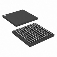
DS21Q48 Maxim Integrated Products, DS21Q48 Datasheet - Page 19

DS21Q48
Manufacturer Part Number
DS21Q48
Description
IC LIU E1/T1/J1 QUAD 5V 144-BGA
Manufacturer
Maxim Integrated Products
Type
Line Interface Units (LIUs)r
Specifications of DS21Q48
Protocol
E1
Voltage - Supply
4.75 V ~ 5.25 V
Mounting Type
Surface Mount
Package / Case
144-CSBGA
Lead Free Status / RoHS Status
Contains lead / RoHS non-compliant
Number Of Drivers/receivers
-
Available stocks
Company
Part Number
Manufacturer
Quantity
Price
Note 1: G.703 requires an accuracy of ±50ppm for both T1 and E1. TR62411 and ANSI specs require an accuracy of ±32ppm for T1
interfaces.
TX0/TX1
RT0/RT1
RRING
SCLKE
NAME
TRING
TNEG
RCLK
RNEG
NRZE
PBEO
TCLK
RPOS
RTIP/
TEST
TPOS
TTIP/
VSM
RCL
TPD
V
V
DD
SS
44/23
27/28
34/37
14/15
21/36
22/35
PIN
42
24
40
25
39
38
43
26
13
41
20
3
4
I/O
O
O
O
O
O
O
I
I
I
I
I
I
I
I
I
I
-
I
-
NRZ Enable [H/W Mode]
0 = Bipolar data at RPOS/RNEG and TPOS/TNEG
1 = NRZ data at RPOS and TPOS or TNEG; RNEG outputs a positive going
pulse when device receives a BPV, CV, or EXZ.
PRBS Bit Error Output. The receiver will constantly search for a QRSS (T1)
or a 2
high if out of synchronization with the PRBS pattern. Goes low when
synchronized to the PRBS pattern. Any errors in the received pattern after
synchronization will cause a positive going pulse (with same period as E1 or T1
clock) synchronous with RCLK.
Receive Clock. Buffered recovered clock from the line. Synchronous to MCLK
in absence of signal at RTIP and RRING.
Receive Carrier Loss. An output which will toggle high during a receive carrier
loss.
Receive Negative Data. Updated on the rising edge (CES = 0) or the falling
edge (CES = 1) of RCLK with the bipolar data out of the line interface. Set
NRZE to a one for NRZ applications. In NRZ mode, data will be output on
RPOS while a received error will cause a positive-going pulse synchronous with
RCLK at RNEG. See Section
Receive Positive Data. Updated on the rising edge (CES = 0) or the falling edge
(CES = 1) of RCLK with bipolar data out of the line interface. Set NRZE pin to a
one for NRZ applications. In NRZ mode, data will be output on RPOS while a
received error will cause a positive-going pulse synchronous with RCLK at
RNEG. See Section
Receive LIU Termination Select Bits 0 & 1 [H/W Mode]. These inputs
determine the receive termination. See
Receive Tip and Ring. Analog inputs for clock recovery circuitry. These pins
connect via a 1:1 transformer to the line. See Section
Receive & Transmit Synchronization Clock Enable.
0 = disable 2.048MHz synchronization transmit and receive mode
1 = enable 2.048MHz synchronization transmit and receive mode
Transmit Clock. A 2.048MHz or 1.544MHz primary clock. Used to clock data
through the transmit side formatter.
Tri-State Control. Set high to tri-state all outputs and I/O pins (including the
parallel control port). Set low for normal operation. Useful in board level testing.
Transmit Negative Data. Sampled on the falling edge (CES = 0) or the rising
edge (CES = 1) of TCLK for data to be transmitted out onto the line.
Transmit Power-Down
0 = normal transmitter operation
1 = powers down the transmitter and tri-states the TTIP and TRING pins
Transmit Positive Data. Sampled on the falling edge (CES = 0) or the rising
edge (CES = 1) of TCLK for data to be transmitted out onto the line.
Transmit Tip and Ring. Analog line driver outputs. These pins connect via a
step-up transformer to the line. See Section
Transmit Data Source Select Bits 0 & 1 [H/W Mode]. These inputs determine
the source of the transmit data. See
5.0V ±5% Positive Supply
Voltage Supply Mode. Should be tied high for 5V operation
Signal Ground
15
-1 (E1) PRBS depending on whether T1 or E1 mode is selected. Remains
19 of 73
6.4
for details.
6.4
for details.
FUNCTION
Table
Table
2-9.
5
2-12.
for details.
5
for details.


