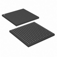
DS26528GN+ Maxim Integrated Products, DS26528GN+ Datasheet - Page 138

DS26528GN+
Manufacturer Part Number
DS26528GN+
Description
IC TXRX T1/E1/J1 OCT 256-CSBGA
Manufacturer
Maxim Integrated Products
Type
Transceiverr
Datasheet
1.DS26528G.pdf
(276 pages)
Specifications of DS26528GN+
Number Of Drivers/receivers
4/4
Protocol
IEEE 1149.1
Voltage - Supply
3.135 V ~ 3.465 V
Mounting Type
Surface Mount
Package / Case
256-CSBGA
Lead Free Status / RoHS Status
Lead free / RoHS Compliant
- Current page: 138 of 276
- Download datasheet (2Mb)
Register Name:
Register Description:
Register Address:
Bit #
Name
Default
Note: This register has an alternate definition for T1 mode. See T1RSLC2.
Bit 7: International Bit (Si).
Bit 6: Frame Non-Alignment Signal Bit (1).
Bit 5: Remote Alarm (A).
Bit 4: Additional Bit 4 (Sa4).
Bit 3: Additional Bit 5 (Sa5).
Bit 2: Additional Bit 6 (Sa6).
Bit 1: Additional Bit 7 (Sa7).
Bit 0: Additional Bit 8 (Sa8).
Register Name:
Register Description:
Register Address:
Bit #
Name
Default
Note: This register has an alternate definition for T1 mode. See T1RSLC3.
Bit 7: Si Bit of Frame 14 (SiF14).
Bit 6: Si Bit of Frame 12 (SiF12).
Bit 5: Si Bit of Frame 10 (SiF10).
Bit 4: Si Bit of Frame 8 (SiF8).
Bit 3: Si Bit of Frame 6 (SiF6).
Bit 2: Si Bit of Frame 4 (SiF4).
Bit 1: Si Bit of Frame 2 (SiF2).
Bit 0: Si Bit of Frame 0 (SiF0).
SiF14
Si
7
0
7
0
E1RNAF (E1 Mode)
E1 Receive Non-Align Frame Register
065h + (200h x n): where n = 0 to 7, for Ports 1 to 8
E1RSiAF (E1 Mode)
E1 Received Si Bits of the Align Frame Register
066h + (200h x n): where n = 0 to 7, for Ports 1 to 8
SiF12
6
1
0
6
0
SiF10
A
5
0
5
0
138 of 276
SiF8
Sa4
4
0
4
0
SiF6
Sa5
3
0
3
0
DS26528 Octal T1/E1/J1 Transceiver
SiF4
Sa6
2
0
2
0
SiF2
Sa7
1
0
1
0
SiF0
Sa8
0
0
0
0
Related parts for DS26528GN+
Image
Part Number
Description
Manufacturer
Datasheet
Request
R

Part Number:
Description:
Network Controller & Processor ICs Octal E1-T1-J1 Singl e-Chip Transceiver (
Manufacturer:
Maxim Integrated Products
Datasheet:

Part Number:
Description:
Network Controller & Processor ICs Octal E1-T1-J1 Singl e-Chip Transceiver (
Manufacturer:
Maxim Integrated Products
Datasheet:

Part Number:
Description:
power light source LUXEON� Collimator
Manufacturer:
LUMILEDS [Lumileds Lighting Company]
Datasheet:

Part Number:
Description:
MAX7528KCWPMaxim Integrated Products [CMOS Dual 8-Bit Buffered Multiplying DACs]
Manufacturer:
Maxim Integrated Products
Datasheet:

Part Number:
Description:
Single +5V, fully integrated, 1.25Gbps laser diode driver.
Manufacturer:
Maxim Integrated Products
Datasheet:

Part Number:
Description:
Single +5V, fully integrated, 155Mbps laser diode driver.
Manufacturer:
Maxim Integrated Products
Datasheet:

Part Number:
Description:
VRD11/VRD10, K8 Rev F 2/3/4-Phase PWM Controllers with Integrated Dual MOSFET Drivers
Manufacturer:
Maxim Integrated Products
Datasheet:

Part Number:
Description:
Highly Integrated Level 2 SMBus Battery Chargers
Manufacturer:
Maxim Integrated Products
Datasheet:

Part Number:
Description:
Current Monitor and Accumulator with Integrated Sense Resistor; ; Temperature Range: -40°C to +85°C
Manufacturer:
Maxim Integrated Products

Part Number:
Description:
TSSOP 14/A�/RS-485 Transceivers with Integrated 100O/120O Termination Resis
Manufacturer:
Maxim Integrated Products

Part Number:
Description:
TSSOP 14/A�/RS-485 Transceivers with Integrated 100O/120O Termination Resis
Manufacturer:
Maxim Integrated Products

Part Number:
Description:
QFN 16/A�/AC-DC and DC-DC Peak-Current-Mode Converters with Integrated Step
Manufacturer:
Maxim Integrated Products

Part Number:
Description:
TDFN/A/65V, 1A, 600KHZ, SYNCHRONOUS STEP-DOWN REGULATOR WITH INTEGRATED SWI
Manufacturer:
Maxim Integrated Products

Part Number:
Description:
Integrated Temperature Controller f
Manufacturer:
Maxim Integrated Products


