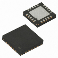
ATA6621-PGQW Atmel, ATA6621-PGQW Datasheet - Page 4

ATA6621-PGQW
Manufacturer Part Number
ATA6621-PGQW
Description
IC TXRX LIN BUS 5V/50MA 20QFN
Manufacturer
Atmel
Type
Transceiverr
Datasheet
1.ATA6621N-PGPW.pdf
(28 pages)
Specifications of ATA6621-PGQW
Number Of Drivers/receivers
1/1
Protocol
LIN
Voltage - Supply
5 V ~ 18 V
Mounting Type
Surface Mount
Package / Case
20-QFN Exposed Pad
Lead Free Status / RoHS Status
Lead free / RoHS Compliant
Available stocks
Company
Part Number
Manufacturer
Quantity
Price
Company:
Part Number:
ATA6621-PGQW
Manufacturer:
AVAGO
Quantity:
349
3. Functional Description
3.1
3.2
3.3
3.4
3.5
3.6
4
Physical Layer Compatibility
Supply Pin (VS)
Ground Pin (GND)
Undervoltage Reset Output (NRES)
Voltage Regulator Output Pin (VCC)
Voltage Regulator Sense Pin (PVCC)
ATA6621N
Since the LIN physical layer is independent from higher LIN layers (e.g., the LIN protocol layer),
all nodes with a LIN physical layer according to revision 2.0 can be mixed with LIN physical layer
nodes, which, according to older versions (i.e., LIN 1.0, LIN 1.1, LIN 1.2, LIN 1.3), are without
any restrictions.
The LIN operating voltage is V
Pre-normal mode and the voltage regulator is switched on (that is, 5V/50 mA output capability).
The supply current in Sleep mode is typically 10 µA, and 40 µA in Silent mode.
The IC is neutral on the LIN pin in case of GND disconnection; it can handle a ground shift up to
3V for supply voltage at the VS pin above 9V.
This push-pull output is supplied from the V
voltage detection threshold of V
except the IC is switched into Sleep mode. Even if V
internally driven from the V
then becomes highly resistant.
The implemented undervoltage delay keeps NRES low for t
normal value.
The internal 5V voltage regulator is capable of driving loads with up to 50 mA of current con-
sumption; it is able to supply the microcontroller and other ICs on the PCB. It is protected
against overloads by means of current limitation and overtemperature shutdown. Furthermore,
the output voltage is monitored and will cause a reset signal at the NRES output pin if the output
voltage drops below a defined threshold V
nal NPN transistor may be used with its base connected to the VCC pin and its emitter
connected to PVCC.
This is the sense input pin of the 5V voltage regulator. For normal applications (that is, when
only using the internal output transistor), this pin is connected to the VCC pin. If an external
boosting transistor is used, the PVCC pin must be connected to the output of this transistor, its
emitter terminal.
S
voltage. If V
thun
S
= 5V to 18V. After switching on VS, the IC starts with the
, NRES switches to low after t
S
thun
voltage ramps down, NRES stays until V
CC
. To boost up the maximum load current, an exter-
voltage. If the V
CC
= 0V the NRES stays low, because it is
Reset
CC
= 10 ms after V
voltage falls below the under-
res_f
(Figure 3-7 on page
4887I–AUTO–09/09
CC
S
reaches its
< 1.5V and
13)


