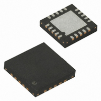
ATA6621-PGQW Atmel, ATA6621-PGQW Datasheet - Page 5

ATA6621-PGQW
Manufacturer Part Number
ATA6621-PGQW
Description
IC TXRX LIN BUS 5V/50MA 20QFN
Manufacturer
Atmel
Type
Transceiverr
Datasheet
1.ATA6621N-PGPW.pdf
(28 pages)
Specifications of ATA6621-PGQW
Number Of Drivers/receivers
1/1
Protocol
LIN
Voltage - Supply
5 V ~ 18 V
Mounting Type
Surface Mount
Package / Case
20-QFN Exposed Pad
Lead Free Status / RoHS Status
Lead free / RoHS Compliant
Available stocks
Company
Part Number
Manufacturer
Quantity
Price
Company:
Part Number:
ATA6621-PGQW
Manufacturer:
AVAGO
Quantity:
349
3.7
3.8
3.9
3.10
3.11
3.12
4887I–AUTO–09/09
Bus Pin (LIN)
Input/Output Pin (TXD)
TXD Dominant Time-out Function
Enable Input Pin (EN)
Wake Input Pin (WAKE)
Output Pin (RXD)
A low side driver with internal current limitation and thermal shutdown, and an internal pull-up
resistor in compliance with LIN specification 2.0 is implemented. This is a self-adapting current
limitation; that is, during current limitation, as the chip temperature increases, the current
decreases. The allowed voltage range is between –40V and +60V. Reverse currents from the
LIN bus to VS are suppressed, even in case of ground shifts or battery disconnection. LIN
receiver thresholds are compatible to the LIN protocol specification. The fall time from recessive
bus state to dominant, and the rise time from dominant bus state to recessive are slope
controlled.
This pin is the microcontroller interface to control the state of the LIN output. TXD must be pulled
to ground in order to have the LIN bus low. If TXD is high, the LIN output transistor is turned off
and the bus is in the recessive state, pulled up by the internal resistor.
The TXD input has an internal pull-up resistor. An internal timer prevents the bus line from being
driven permanently in the dominant state. If TXD is forced to low longer than t
LIN bus driver is switched to the recessive state. To reset this dominant time-out mode, TXD
must be switched to high (> 10 µs) before normal data transmission can be started.
This pin reports the state of the LIN bus to the microcontroller. LIN high (recessive state) is
reported by a high level at RXD, LIN low (dominant state) is reported by a low level at RXD. The
output has an internal pull-up structure with typically 5 k to V
defined with an external load capacitor of 20 pF.
The output is short-circuit protected. In Unpowered mode (that is, V
This pin controls the operation mode of the interface. If EN is high, the interface is in Normal
mode, with transmission paths from TXD to LIN and from LIN to RXD both being active. The V
voltage regulator is operating with 5V ±2%/50 mA output capability.
If EN is switched to low while TXD is still high, the device is forced to Silent mode. No data trans-
mission is then possible and the current consumption is reduced to I
capability of the V
If EN is switched to low while TXD is low, the device is forced to Sleep mode. No data transmis-
sion is possible and the voltage regulator is switched off.
This pin is a high voltage input used to wake the device up from Sleep mode. It is usually con-
nected to an external switch in the application to generate a local wake-up. A pull-up current
source with typically 10 µA is implemented.
If you don’t need a local wake-up in your application, connect pin WAKE directly to pin VS.
CC
regulator is also 50 mA, but the V
CC
tolerance is between 4.65V and 5.35V.
CC
. The AC characteristics can be
S
= 0V), RXD is switched off.
VS
= 50 µA. The current
ATA6621N
DOM
> 6 ms, the
CC
5


