AD8392ARE Analog Devices Inc, AD8392ARE Datasheet - Page 5
AD8392ARE
Manufacturer Part Number
AD8392ARE
Description
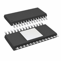
IC LINE DRVR ADSL/ADSL2 28TSSOP
Manufacturer
Analog Devices Inc
Type
Driverr
Datasheet
1.AD8392AREZ-REEL.pdf
(16 pages)
Specifications of AD8392ARE
Number Of Drivers/receivers
2/0
Protocol
xDSL
Voltage - Supply
5 V ~ 24 V
Mounting Type
Surface Mount
Package / Case
28-TSSOP Exposed Pad, 28-eTSSOP, 28-HTSSOP
Power Supply Requirement
Single/Dual
Package Type
TSSOP EP
Slew Rate
900V/us
Pin Count
28
Lead Free Status / RoHS Status
Contains lead / RoHS non-compliant
Available stocks
Company
Part Number
Manufacturer
Quantity
Price
Company:

Part Number:
AD8392ARE
Manufacturer:
AD
Quantity:
5 510
Company:
Part Number:
AD8392ARE
Manufacturer:
TOS
Quantity:
5 510
Part Number:
AD8392AREZ
Manufacturer:
ADI/亚德诺
Quantity:
20 000


ABSOLUTE MAXIMUM RATINGS
Table 3.
Parameter
Supply Voltage
Power Dissipation
Storage Temperature
Operating Temperature Range
Lead Temperature Range (Soldering 10 sec)
Junction Temperature
Stresses above those listed under Absolute Maximum Ratings
may cause permanent damage to the device. This is a stress
rating only; functional operation of the device at these or any
other conditions above those indicated in the operational
section of this specification is not implied. Exposure to absolute
maximum rating conditions for extended periods may affect
device reliability.
THERMAL RESISTANCE
θ
for device soldered in circuit board for surface-mount packages.
Table 4. Thermal Resistance
Package Type
LFCSP-32 (CP)
TSSOP-28/EP (RE)
Maximum Power Dissipation
The power dissipated in the package (P
quiescent power dissipation and the power dissipated in the
package due to the load drive for all outputs. The quiescent
power is the voltage between the supply pins (V
quiescent current (I
the total drive power is V
dissipated in the package and some in the load (V
ESD CAUTION
ESD (electrostatic discharge) sensitive device. Electrostatic charges as high as 4000 V readily accumulate on the
human body and test equipment and can discharge without detection. Although this product features proprie-
tary ESD protection circuitry, permanent damage may occur on devices subjected to high energy electrostatic
discharges. Therefore, proper ESD precautions are recommended to avoid performance degradation or loss of
functionality.
JA
is specified for the worst-case conditions, i.e., θ
S
). Assuming that the load (R
S
/2 × I
OUT
, some of which is
D
θ
27.27
35.33
) is the sum of the
JA
Rating
±13 V (+26 V)
See Figure 3
−65°C to +150°C
−40°C to +85°C
300°C
150°C
S
) times the
L
) is midsupply,
OUT
JA
is specified
× I
Unit
°C/W
°C/W
OUT
).
Rev. A | Page 5 of 16
RMS output voltages should be considered. If R
to V
In single supply with R
Airflow increases heat dissipation, effectively reducing θ
more metal directly in contact with the package leads from
metal traces, through holes, ground, and power planes reduces
the θ
Figure 3 shows the maximum safe power dissipation in the
package versus the ambient temperature for the LFCSP-32 and
TSSOP-28/EP packages on a JEDEC standard 4-layer board. θ
values are approximations.
See the Thermal Considerations section for additional thermal
design guidance.
Figure 3. Maximum Power Dissipation vs. Temperature for a 4-Layer Board
S−
JA
.
as in single-supply operation, the total power is V
7
6
5
4
3
2
1
0
–40 –30 –20 –10
TSSOP-28/EP
L
0
to V
TEMPERATURE (°C)
10
S−
20
, worst case is V
30
LFCSP-32
40
50
60
OUT
T
L
J
70
= 150°C
is referenced
= V
80
AD8392
S
/2.
90
S
JA
× I
. Also,
OUT
JA
.
Related parts for AD8392ARE
Image
Part Number
Description
Manufacturer
Datasheet
Request
R

Part Number:
Description:
±1.7g Dual-Axis IMEMS Accelerometer Evaluation Board
Manufacturer:
Analog Devices Inc
Datasheet:

Part Number:
Description:
Inertial Sensor Evaluation System
Manufacturer:
Analog Devices Inc
Datasheet:
Part Number:
Description:
Manufacturer:
Analog Devices Inc
Datasheet:
Part Number:
Description:
Manufacturer:
Analog Devices Inc
Datasheet:
Part Number:
Description:
Manufacturer:
Analog Devices Inc
Datasheet:
Part Number:
Description:
Manufacturer:
Analog Devices Inc
Datasheet:
Part Number:
Description:
Manufacturer:
Analog Devices Inc
Datasheet:
Part Number:
Description:
Manufacturer:
Analog Devices Inc
Datasheet:
Part Number:
Description:
Manufacturer:
Analog Devices Inc
Datasheet:
Part Number:
Description:
Manufacturer:
Analog Devices Inc
Datasheet:
Part Number:
Description:
Manufacturer:
Analog Devices Inc
Datasheet:
Part Number:
Description:
Manufacturer:
Analog Devices Inc
Datasheet:
Part Number:
Description:
Manufacturer:
Analog Devices Inc
Datasheet: