JN5148/001M00T,534 NXP Semiconductors, JN5148/001M00T,534 Datasheet - Page 8
JN5148/001M00T,534
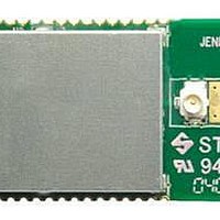
Manufacturer Part Number
JN5148/001M00T,534
Description
Microcontrollers (MCU) 32bit RISC 32MHz
Manufacturer
NXP Semiconductors
Datasheet
1.JN5148001M00T534.pdf
(23 pages)
Specifications of JN5148/001M00T,534
Processor Series
JN5148
Core
RISC
Data Bus Width
32 bit
Data Ram Size
128 KB
Interface Type
JTAG, 2-Wire Serial, 4-Wire Digital Audio, I2S
Maximum Clock Frequency
32 MHz
Maximum Operating Temperature
+ 85 C
Mounting Style
SMD/SMT
Minimum Operating Temperature
- 40 C
Core Architecture
RISC
Lead Free Status / Rohs Status
Details
Other names
935294034534


33
34
35
36
37
38
39
40
41
*: These two pins are not connected for High power modules
4.2. Pin Descriptions
All pins behave as described in the JN-DS-JN5148 Wireless Microcontroller Datasheet [2], with the exception of the
following:
4.2.1 Power Supplies
A single power supply pin, VDD is provided. Separate analogue (VSSA) and digital (GND) grounds are provided.
These should be connected together at the module pins.
4.2.2 SPI Memory Connections
SPISWP is a write protect pin for the serial flash memory. This should be held low to inhibit writes to the flash device.
SPISSZ is connected to SPI Slave Select 0 on the JN5148.
SPISSM is connected to the Slave Select pin on the memory.
This configuration allows the flash memory device to be programmed using an external SPI programmer if required.
For programming in this mode, the JN5148 should be held in reset by taking RESETN low. Two potential flash 4Mbit
memory devices may be used in the module, the Numonyx M25P40 and the SST SST25VF040B.
The memory can also be programmed over the UART by using the flash programmer software provided by Jennic.
This is available as part of the Software Developer kit and libraries available from www.nxp.com/jennic. To enter
this programming mode, SPIMISO (pin 7) should be held low whilst the chip is reset. Once programming has finished,
the chip should be reset, when it will execute the new code downloaded.
For normal operation of the module and programming over the UART, SPISSZ should be connected to
SPISSM.
8
COMP1+
COMP1-
DIO 20
DIO17
DIO18
DIO19
ADC1
ADC2
ADC3
CTS1
RTS1
TXD1
RXD1
IP_SEL
IP_INT
JN-DS-JN5148-001-Myy 1v4
DAI_SDOUT
DAI_SCK
JTAG_TMS
JTAG_TDO
JTAG_TCK
JTAG_TDI
CMOS
CMOS
CMOS
CMOS
3.3V
3.3V
3.3V
3.3V
3.3V
DIO17, UART 1 Clear To Send
Input, Intelligent Peripheral Device
Select Input or Digital Audio Clock
or JTAG CLK
DIO18, UART 1 Request To Send
Output, Intelligent Peripheral
Interrupt Output or Digital Audio
Data Output or JTAG Mode Select
DIO19 or UART 1 Transmit Data
Output or JTAG Data Out
DIO 20, UART 1 Receive Data
Input or JTAG data In
Comparator 1 Input -ve
Comparator 1 Input +ve
Analogue to Digital Input
Analogue to Digital Input
Analogue to Digital Input
© NXP Laboratories UK 2010
Related parts for JN5148/001M00T,534
Image
Part Number
Description
Manufacturer
Datasheet
Request
R

Part Number:
Description:
Microcontrollers (MCU) 32bit RISC 2.4GHz
Manufacturer:
NXP Semiconductors
Datasheet:

Part Number:
Description:
IC MCU 802.15.4 32BIT 2.4G 56QFN
Manufacturer:
NXP Semiconductors
Datasheet:

Part Number:
Description:
MODULE ZIGBEE PRO U.FL CONN
Manufacturer:
NXP Semiconductors
Datasheet:

Part Number:
Description:
MODULE ZIGBEE PRO CERM ANTENNA
Manufacturer:
NXP Semiconductors
Datasheet:

Part Number:
Description:
MODULE ZIGBEE PRO HP U.FL CONN
Manufacturer:
NXP Semiconductors
Datasheet:

Part Number:
Description:
MCU 802.15.4 32BIT 2.4G 56-QFN
Manufacturer:
NXP Semiconductors
Datasheet:
Part Number:
Description:
MCU 802.15.4 32BIT 2.4G 56-QFN
Manufacturer:
NXP Semiconductors
Datasheet:
Part Number:
Description:
NXP Semiconductors designed the LPC2420/2460 microcontroller around a 16-bit/32-bitARM7TDMI-S CPU core with real-time debug interfaces that include both JTAG andembedded trace
Manufacturer:
NXP Semiconductors
Datasheet:

Part Number:
Description:
NXP Semiconductors designed the LPC2458 microcontroller around a 16-bit/32-bitARM7TDMI-S CPU core with real-time debug interfaces that include both JTAG andembedded trace
Manufacturer:
NXP Semiconductors
Datasheet:
Part Number:
Description:
NXP Semiconductors designed the LPC2468 microcontroller around a 16-bit/32-bitARM7TDMI-S CPU core with real-time debug interfaces that include both JTAG andembedded trace
Manufacturer:
NXP Semiconductors
Datasheet:
Part Number:
Description:
NXP Semiconductors designed the LPC2470 microcontroller, powered by theARM7TDMI-S core, to be a highly integrated microcontroller for a wide range ofapplications that require advanced communications and high quality graphic displays
Manufacturer:
NXP Semiconductors
Datasheet:
Part Number:
Description:
NXP Semiconductors designed the LPC2478 microcontroller, powered by theARM7TDMI-S core, to be a highly integrated microcontroller for a wide range ofapplications that require advanced communications and high quality graphic displays
Manufacturer:
NXP Semiconductors
Datasheet:
Part Number:
Description:
The Philips Semiconductors XA (eXtended Architecture) family of 16-bit single-chip microcontrollers is powerful enough to easily handle the requirements of high performance embedded applications, yet inexpensive enough to compete in the market for hi
Manufacturer:
NXP Semiconductors
Datasheet:
Part Number:
Description:
The XA-S3 device is a member of Philips Semiconductors? XA(eXtended Architecture) family of high performance 16-bitsingle-chip microcontrollers
Manufacturer:
NXP Semiconductors
Datasheet: