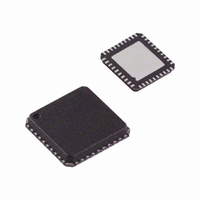
ADV7179BCPZ Analog Devices Inc, ADV7179BCPZ Datasheet - Page 4

ADV7179BCPZ
Manufacturer Part Number
ADV7179BCPZ
Description
IC ENCODER VID NTSC/PAL 40LFCSP
Manufacturer
Analog Devices Inc
Type
Video Encoderr
Datasheet
1.ADV7179KCPZ.pdf
(52 pages)
Specifications of ADV7179BCPZ
Applications
Digital Cameras, Mobile Phones, Portable Video
Voltage - Supply, Analog
2.8 V, 3.3 V
Mounting Type
Surface Mount
Package / Case
40-LFCSP
Input Format
Digital
Output Format
Analog
Supply Voltage Range
3V To 3.6V
Operating Temperature Range
-40°C To +85°C
Tv / Video Case Style
LFCSP
No. Of Pins
40
Msl
MSL 1 - Unlimited
Lead Free Status / RoHS Status
Lead free / RoHS Compliant
Voltage - Supply, Digital
-
Lead Free Status / RoHS Status
Lead free / RoHS Compliant, Lead free / RoHS Compliant
Available stocks
Company
Part Number
Manufacturer
Quantity
Price
Company:
Part Number:
ADV7179BCPZ
Manufacturer:
ADI
Quantity:
230
Part Number:
ADV7179BCPZ
Manufacturer:
ADI/亚德诺
Quantity:
20 000
Company:
Part Number:
ADV7179BCPZ-REEL
Manufacturer:
XILINX
Quantity:
1 150
ADV7174/ADV7179
SPECIFICATIONS
2.8 V SPECIFICATIONS
V
Table 1.
Parameter
STATIC PERFORMANCE
DIGITAL INPUTS
DIGITAL OUTPUTS
ANALOG OUTPUTS
POWER REQUIREMENTS
1
2
3
4
5
6
7
8
Temperature range T
reduces I
Total DAC current in sleep mode.
Total continuous current during sleep mode.
Guaranteed by characterization.
DACs can output 35 mA typically at 2.8 V (R
Power measurements are taken with clock frequency = 27 MHz. Max T
I
I
DAC
CCT
AA
Resolution (Each DAC)
Accuracy (Each DAC)
Input High Voltage, V
Input Low Voltage, V
Input Current, I
Input Capacitance, C
Output High Voltage, V
Output Low Voltage, V
Three-State Leakage Current
Three-State Output Capacitance
Output Current
DAC-to-DAC Matching
Output Compliance, V
Output Impedance, R
Output Capacitance, C
V
Normal Power Mode
Low Power Mode
Sleep Mode
Power Supply Rejection Ratio
AA
(circuit current) is the continuous current required to drive the device.
is the total current (min corresponds to 5 mA output per DAC, max corresponds to 37 mA output per DAC) to drive all three DACs. Turning off individual DACs
= 2.8 V, V
Integral Nonlinearity
Differential Nonlinearity
I
I
I
I
I
I
DAC
CCT
DAC
CCT
DAC
CCT
6
6
8
7
DAC
(Max)
(Max)
correspondingly.
REF
5
5
2
= 1.235 V, R
IN
2
3
MIN
2
to T
2
INL
IN
INH
OUT
2, 4
MAX
OC
OUT
OL
OH
: –20°C to +85°C.
SET
= 150 Ω. All specifications T
SET
= 150 Ω and R
L
= 37.5 Ω). Full drive into 37.5 Ω load.
Conditions
R
Guaranteed monotonic
V
I
I
R
I
R
COMP = 0.1 μF
SOURCE
SINK
OUT
SET
SET
SET
IN
= 0.4 V or 2.4 V
= 0 mA
= 300 Ω
= 3.2 mA
= 150 Ω, R
= 150 Ω, R
J
= 110°C.
MIN
= 400 μA
Rev. B | Page 4 of 52
to T
1
MAX
L
L
= 37.5 Ω
= 37.5 Ω
1
, unless otherwise noted.
Min
1.6
2.4
33
0
2.8
Typ
±3.0
10
10
34.7
2.0
30
115
30
62
30
0.1
0.001
0.01
Max
10
±1
0.7
±1
0.4
10
37
1.4
30
120
0.5
Bits
Unit
LSB
LSB
V
V
μA
pF
V
V
μA
pF
mA
%
V
kΩ
pF
V
mA
mA
mA
mA
μA
μA
%/%


