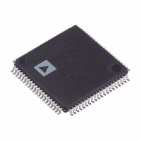
ADV7194KSTZ Analog Devices Inc, ADV7194KSTZ Datasheet - Page 38

ADV7194KSTZ
Manufacturer Part Number
ADV7194KSTZ
Description
IC ENCODER VIDEO EXT-10 80-LQFP
Manufacturer
Analog Devices Inc
Type
Video Encoderr
Datasheet
1.ADV7194KSTZ.pdf
(69 pages)
Specifications of ADV7194KSTZ
Applications
DVD, PC Video, Multimedia
Voltage - Supply, Analog
3.3 V ~ 5 V
Voltage - Supply, Digital
3.3 V ~ 5 V
Mounting Type
Surface Mount
Package / Case
80-LQFP
Input Format
Digital
Output Format
Analog
Supply Voltage Range
3.15V To 3.6V
Operating Temperature Range
0°C To +70°C
Tv / Video Case Style
LQFP
No. Of Pins
80
Msl
MSL 1 - Unlimited
Svhc
No SVHC
Rohs Compliant
Yes
Lead Free Status / RoHS Status
Lead free / RoHS Compliant
For Use With
EVAL-ADV7194EB - BOARD EVAL FOR ADV7194
Lead Free Status / RoHS Status
Lead free / RoHS Compliant, Lead free / RoHS Compliant
Available stocks
Company
Part Number
Manufacturer
Quantity
Price
Company:
Part Number:
ADV7194KSTZ
Manufacturer:
ADI
Quantity:
393
Company:
Part Number:
ADV7194KSTZ
Manufacturer:
ADI
Quantity:
717
Company:
Part Number:
ADV7194KSTZ
Manufacturer:
Analog Devices Inc
Quantity:
10 000
Part Number:
ADV7194KSTZ
Manufacturer:
ADI/亚德诺
Quantity:
20 000
ADV7194
TELETEXT REQUEST CONTROL REGISTER TC07
(TC07–TC00)
(Address (SR4–SR0) = 1CH)
Teletext Control Register is an 8-bit-wide register. See Figure
74.
TTXREQ Falling Edge Control (TC00–TC03)
These bits control the position of the falling edge of TTXREQ.
It can be programmed from zero clock cycles to a maximum of 15
clock cycles. This controls the active window for Teletext data.
Increasing this value reduces the amount of Teletext bits below the
default of 360. If Bits TC00–TC03 are 00Hex when Bits TC04–
TC07 are changed then the falling edge of TTREQ will track that
of the rising edge (i.e., the time between the falling and rising
edge remains constant).
PCLK = clock cycle at 27 MHz.
FIELD 1/3
FIELD 2/4
FIELD 1/3
FIELD 2/4
FIELD 1/3
FIELD 1/3
FIELD 2/4
FIELD 2/4
PCO15 PCO14 PCO13 PCO12 PCO11 PCO10
LINE 17 LINE 16
LINE 25 LINE 24 LINE 23
LINE 17 LINE 16
LINE 25 LINE 24 LINE 23
PCE15
LINE 14 LINE 13
LINE 22 LINE 21 LINE 20
LINE 14 LINE 13
LINE 22 LINE 21 LINE 20
TXO15
TXE15
PCO7
PCE7
TXO7
TXE7
PCE14
TXO14
PCO6
TXE14
PCE6
TXO6
TXE6
LINE 15 LINE 14 LINE 13 LINE 12 LINE 11 LINE 10
LINE 15 LINE 14 LINE 13 LINE 12 LINE 11 LINE 10
PCE13
LINE 12 LINE 11 LINE 10
TXO13
LINE 12 LINE 11 LINE 10
TXE13
PCO5
PCE5
TXO5
TXE5
C/W07
WWS CONTROL
0
1
LINE 22 LINE 21 LINE 20
LINE 22 LINE 21 LINE 20
PCE12
LINE 19 LINE 18 LINE 17
LINE 19 LINE 18 LINE 17
TXO12
TXE12
PCO4
PCE4
TXO4
TXE4
C/W07
DISABLE
ENABLE
C/W06
PCE11
CGMS EVEN FIELD
TXO11
TXE11
PCO3
PCE3
TXO3
TXE3
0
1
CONTROL
C/W06
DISABLE
ENABLE
PCE10
TXO10
TXE10
PCO2
PCE2
LINE 9
LINE 9
TXO2
TXE2
C/W05
CGMS ODD FIELD
0
1
LINE 19 LINE 18
CONTROL
LINE 19 LINE 18
LINE 16 LINE 15
LINE 16 LINE 15
PCO1
PCO9
PCE1
PCE9
LINE 8
LINE 8
TXO9
TXO1
TXE1
TXE9
C/W05
DISABLE
ENABLE
C/W04
CGMS CRC CHECK
LINE 7
LINE 7
PCO0
PCO8
PCE0
PCE8
TXO8
TXO0
TXE0
TXE8
0
1
CONTROL
C/W04
DISABLE
ENABLE
TTXREQ Rising Edge Control (TC04–TC07)
These bits control the position of the rising edge of TTXREQ.
It can be programmed from zero clock cycles to a maximum of 15
clock cycles.
PCLK = clock cycle at 27 MHz.
CGMS_WSS REGISTER 0 C/W0 (C/W07–C/W00)
(Address (SR4–SR0) = 19H)
CGMS_WSS register 0 is an 8-bit-wide register. Figure 71 shows
the operations under control of this register.
C/W0 BIT DESCRIPTION
CGMS Data (C/W00–C/W03)
These four data bits are the final four bits of CGMS data out-
put stream. Note it is CGMS data ONLY in these bit positions,
i.e., WSS data does not share this location.
CGMS CRC Check Control (C/W04)
When this bit is enabled (1), the last six bits of the CGMS data,
i.e., the CRC check sequence, is internally calculated by the
ADV7194. If this bit is disabled (0), the CRC values in the reg-
ister are output to the CGMS data stream.
CGMS Odd Field Control (C/W05)
When this bit is set (1), CGMS is enabled for odd fields. Note
this is only valid in NTSC mode.
CGMS Even Field Control (C/W06)
When this bit is set (1), CGMS is enabled for even fields. Note
this is only valid in NTSC mode.
WSS Control (C/W07)
When this bit is set (1), wide screen signalling is enabled. Note
this is only valid in PAL mode.
C/W03
TC07
TC07 TC06 TC05 TC04
0
0
''
1
1
RISING EDGE CONTROL
0
0
''
1
1
TC06
C/W02
TTXREQ
C/W03 – C/W00
0
1
1
0
''
CGMS DATA
0
TC05
1
''
0
1
C/W01
0 PCLK
1 PCLK
'' PCLK
14 PCLK
15 PCLK
TC04
C/W00
TC03
TC03 TC02 TC01 TC00
0
0
''
1
1
FALLING EDGE CONTROL
0
0
''
1
1
TC02
TTXREQ
0
0
''
1
1
TC01
0
''
1
0
1
0 PCLK
1 PCLK
'' PCLK
14 PCLK
15 PCLK
TC00


