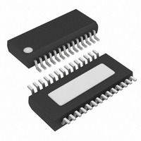
MAX9526AEI+T Maxim Integrated Products, MAX9526AEI+T Datasheet - Page 19

MAX9526AEI+T
Manufacturer Part Number
MAX9526AEI+T
Description
IC VID DECODER NTSC/PAL 28-QSOP
Manufacturer
Maxim Integrated Products
Type
Video Decoderr
Datasheet
1.MAX9526AEI.pdf
(38 pages)
Specifications of MAX9526AEI+T
Applications
Automotive Systems, Players, TV
Voltage - Supply, Analog
1.8V
Voltage - Supply, Digital
1.8V
Mounting Type
Surface Mount
Package / Case
28-QSOP
Lead Free Status / RoHS Status
Lead free / RoHS Compliant
transition on SDA while SCL is high (Figure 11). A START
condition from the master signals the beginning of a
transmission to the MAX9526. The master terminates
transmission, and frees the bus, by issuing a STOP con-
dition. The bus remains active if a REPEATED START
condition is generated instead of a STOP condition.
The MAX9526 recognizes a STOP condition at any
point during data transmission except if the STOP con-
dition occurs in the same high pulse as a START condi-
tion. For proper operation, do not send a STOP
condition during the same SCL high pulse as the
START condition.
The slave address is defined as the seven most signifi-
cant bits (MSBs) followed by the read/write bit. For
DEVADR connected to DGND, setting the read/write bit to
1 (slave address = 0x43) configures the MAX9526 for
read mode. Setting the read/write bit to 0 (slave address
= 0x42) configures the MAX9526 for write mode. The
address is the first byte of information sent to the
MAX9526 after the START condition. The MAX9526 slave
address is configurable with DEVADR. Table 5 shows the
addresses of the MAX9526.
The acknowledge bit (ACK) is a clocked 9th bit that the
MAX9526 uses to handshake receipt each byte of data
when in write mode (see Figure 12). The MAX9526 pulls
down SDA during the entire master-generated 9th clock
pulse if the previous byte is successfully received.
Monitoring ACK allows for detection of unsuccessful
data transfers. An unsuccessful data transfer occurs if
a receiving device is busy or if a system fault has
occurred. In the event of an unsuccessful data transfer,
the bus master retries communication. The master pulls
______________________________________________________________________________________
Early STOP Conditions
Slave Address
Acknowledge
Low-Power, High-Performance
NTSC/PAL Video Decoder
down SDA during the 9th clock cycle to acknowledge
receipt of data when the MAX9526 is in read mode. An
acknowledge is sent by the master after each read byte
to allow data transfer to continue. A not acknowledge is
sent when the master reads the final byte of data from
the MAX9526, followed by a STOP condition.
A write to the MAX9526 includes transmission of a
START condition, the slave address with the R/W bit set
to 0, one byte of data to configure the internal register
address pointer, one or more bytes of data, and a
STOP condition. Figure 13 illustrates the proper frame
format for writing one byte of data to the MAX9526.
Figure 14 illustrates the frame format for writing n bytes
of data to the MAX9526.
The slave address with the R/W bit set to 0 indicates
that the master intends to write data to the MAX9526.
The MAX9526 acknowledges receipt of the address
byte during the master-generated 9th SCL pulse.
The second byte transmitted from the master config-
ures the MAX9526’s internal register address pointer.
The pointer tells the MAX9526 where to write the next
byte of data. An acknowledge pulse is sent by the
MAX9526 upon receipt of the address pointer data.
The third byte sent to the MAX9526 contains the data
that is written to the chosen register. An acknowledge
pulse from the MAX9526 signals receipt of the data
byte. The address pointer autoincrements to the next
register address after each received data byte. This
autoincrement feature allows a master to write to
sequential registers within one continuous frame. Figure
14 illustrates how to write to multiple registers with one
frame. The master signals the end of transmission by
issuing a STOP condition.
Write Data Format
19


