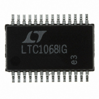
LTC1068IG#PBF Linear Technology, LTC1068IG#PBF Datasheet - Page 10

LTC1068IG#PBF
Manufacturer Part Number
LTC1068IG#PBF
Description
IC FILTR BUILDNG BLK QUAD 28SSOP
Manufacturer
Linear Technology
Datasheet
1.LTC1068CNPBF.pdf
(28 pages)
Specifications of LTC1068IG#PBF
Filter Type
Universal Switched Capacitor
Frequency - Cutoff Or Center
50kHz
Number Of Filters
4
Max-order
8th
Voltage - Supply
3.14 V ~ 11 V, ±3.14 V ~ 5.5 V
Mounting Type
Surface Mount
Package / Case
28-SSOP
Lead Free Status / RoHS Status
Lead free / RoHS Compliant
Available stocks
Company
Part Number
Manufacturer
Quantity
Price
PIN
LTC1068 Series
path. A 200Ω resistor between clock source and Pin 11 will
slow down the rise and fall times of the clock to further
reduce charge coupling (Figures 1 and 2).
Output Pins
Each 2nd order section of an LTC1068 device has three
outputs that typically source 17mA and sink 6mA. Driving
coaxial cables or resistive loads less than 20k will degrade
the total harmonic distortion performance of any filter
design. When evaluating the distortion or noise perfor-
mance of a particular filter design implemented with a
LTC1068 device, the final output of the filter should be
buffered with a wideband, noninverting high slew rate
amplifier (Figure 3).
Inverting Input Pins
These pins are the inverting inputs of internal op amps and
are susceptible to stray capacitive coupling from low
impedance signal outputs and power supply lines.
10
BLOCK
U
FUNCTIONS
U
DIAGRAM
AGND
INV A
INV D
INV B
INV C
(14)
(28)
(15)
U
(7)
(1)
W
–
+
–
+
–
+
–
+
HPC/NC
HPD/ND
HPA/NA
HPB/NB
(27)
(13)
(16)
(2)
+
+
+
+
–
–
–
–
(10)
(24)
(19)
Σ
SA
Σ
SB
(5)
Σ
SC
Σ
SD
+
+
+
+
PIN 28-LEAD SSOP PACKAGE
In a printed circuit layout any signal trace, clock source
trace or power supply trace should be at least 0.1 inches
away from any inverting input pins
Summing Input Pins
These are voltage input pins. If used, they should be driven
with a source impedance below 5k. When they are not
used, they should be tied to the analog ground pin.
The summing pin connections determine the circuit topol-
ogy (mode) of each 2nd order section. Please refer to
Modes of Operation.
BPA
(12)
BPB
BPC
(26)
BPD
(17)
(3)
+
+
+
+
+
(11)
LPA
LPB
LPC
(25)
LPD
(18)
(4)
Figure 3. Wideband Buffer
*THE RATIO R
1k
DEVICE
LTC1068
LTC1068-200
LTC1068-25
LTC1068-50
AGND (7)
–
+
LT
A
R
R
/R
11.3k
®
A
B
10k
R
1354
*
*
B
A
VARIES ± 2%
CLK (21)
V
NC (20)
NC (22)
8.6k
NC (6)
NC (9)
1068 BD
V
10k
R
–
+
B
(23)
(8)
1068 F03
1068fb


