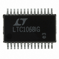
LTC1068IG#PBF Linear Technology, LTC1068IG#PBF Datasheet - Page 9

LTC1068IG#PBF
Manufacturer Part Number
LTC1068IG#PBF
Description
IC FILTR BUILDNG BLK QUAD 28SSOP
Manufacturer
Linear Technology
Datasheet
1.LTC1068CNPBF.pdf
(28 pages)
Specifications of LTC1068IG#PBF
Filter Type
Universal Switched Capacitor
Frequency - Cutoff Or Center
50kHz
Number Of Filters
4
Max-order
8th
Voltage - Supply
3.14 V ~ 11 V, ±3.14 V ~ 5.5 V
Mounting Type
Surface Mount
Package / Case
28-SSOP
Lead Free Status / RoHS Status
Lead free / RoHS Compliant
Available stocks
Company
Part Number
Manufacturer
Quantity
Price
PIN
Power Supply Pins
The V
capacitor to an adequate analog ground. The filter’s power
supplies should be isolated from other digital or high
voltage analog supplies. A low noise linear supply is
recommended. Using a switching power supply will lower
the signal-to-noise ratio of the filter. Figures 1 and 2 show
typical connections for dual and single supply operation.
Analog Ground Pin
The filter’s performance depends on the quality of the
analog signal ground. For either dual or single supply
operation, an analog ground plane surrounding the pack-
age is recommended. The analog ground plane should be
connected to any digital ground at a single point. For single
supply operation, AGND should be bypassed to the analog
ground plane with at least a 0.47µF capacitor (Figure 2).
Two internal resistors bias the analog ground pin. For the
LTC1068, LTC1068-200 and LTC1068-25, the voltage at
the analog ground pin (AGND) for single supply is 0.5 × V
and for the LTC1068-50 it is 0.435 × V
U
ANALOG
GROUND
PLANE
+
FUNCTIONS
Figure 1. Dual Supply Ground Plane Connections
V
0.1µF
and V
+
STAR
SYSTEM
GROUND
U
–
pins should each be bypassed with a 0.1µF
10
11
12
13
14
1
2
3
4
5
6
7
8
9
U
LTC1068
28
27
26
25
24
23
22
21
20
19
18
17
16
15
SOURCE
CLOCK
V
+
–
.
DIGITAL GROUND
0.1µF
200Ω
1068 F01
+
Clock Input Pin
Any TTL or CMOS clock source with a square-wave output
and 50% duty cycle (±10%) is an adequate clock source
for the device. The power supply for the clock source
should not be the filter’s power supply. The analog ground
for the filter should be connected to clock’s ground at a
single point only. Table 2 shows the clock’s low and high
level threshold values for dual or single supply operation.
Table 2. Clock Source High and Low Threshold Levels
POWER SUPPLY
Dual Supply = ±5V
Single Supply = 5V
Single Supply = 3.3V
A pulsed generator can be used as a clock source provided
the high level ON time is at least 25% of the pulse period.
Sine waves are not recommended for clock input frequen-
cies less than 100kHz, since excessively slow clock rise or
fall times generate internal clock jitter (maximum clock
rise or fall time ≤ 1µs). The clock signal should be routed
from the right side of the IC package and perpendicular to
it to avoid coupling to any input or output analog signal
Figure 2. Single Supply Ground Plane Connections
ANALOG
GROUND
PLANE
DEVICE
LTC1068
LTC1068-200
LTC1068-25
LTC1068-50
V
FOR MODE 3, THE S NODE
SHOULD BE TIED TO PIN 7 (AGND)
AGND
STAR
SYSTEM
GROUND
0.47µF
(1µF FOR
STOPBAND
FREQUENCIES
≤ 1kHz)
V
+
0.1µF
11.3k
10k
R
A
8.6k
10k
R
B
HIGH LEVEL
10
11
12
13
14
≥ 1.53V
≥ 1.53V
≥ 1.20V
1
2
3
4
5
6
7
8
9
LTC1068 Series
R
A
LTC1068
R
SOURCE
CLOCK
B
28
27
26
25
24
23
22
21
20
19
18
17
16
15
DIGITAL GROUND
LOW LEVEL
≤ 0.53V
≤ 0.53V
≤ 0.53V
200Ω
1068 F02
1068fb
9


