LTC6601CUF-2#TRPBF Linear Technology, LTC6601CUF-2#TRPBF Datasheet
LTC6601CUF-2#TRPBF
Specifications of LTC6601CUF-2#TRPBF
Available stocks


Related parts for LTC6601CUF-2#TRPBF


LTC6601CUF-2#TRPBF Summary of contents
Page 1
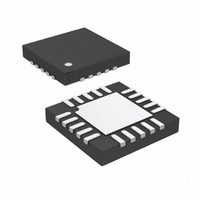
... The LTC6601-2 is available in a compact 4mm × 4mm 20-pin leadless QFN package. L, LT, LTC and LTM are registered trademarks of Linear Technology Corporation. All other trademarks are the property of their respective owners. Protected by U.S. Patents including 6271719. 25MHz Filter, Single-Ended Input, Low Power Mode – ...
Page 2
... ORDER INFORMATION LEAD FREE FINISH TAPE AND REEL LTC6601CUF-2#PBF LTC6601CUF-2#TRPBF LTC6601IUF-2#PBF LTC6601IUF-2#TRPBF Consult LTC Marketing for parts specifi ed with wider operating temperature ranges. *The temperature grade is identifi label on the shipping container. For more information on lead free part marking, go to: For more information on tape and reel specifi ...
Page 3
DC ELECTRICAL CHARACTERISTICS temperature range, otherwise specifi cations are 100k. The fi lter is confi gured for a gain of 1 unless otherwise noted. V LOAD BAL + – )/2. ...
Page 4
LTC6601-2 DC ELECTRICAL CHARACTERISTICS temperature range, otherwise specifi cations are 100k. The fi lter is confi gured for a gain of 1 unless otherwise noted. V LOAD BAL + – ...
Page 5
AC ELECTRICAL CHARACTERISTICS temperature range, otherwise specifi cations are at T fl oating, unless otherwise noted. (See Figure 2 for the AC test confi guration.) V – defi ned OUT ICM INP ...
Page 6
LTC6601-2 ELECTRICAL CHARACTERISTICS Note 1: Stresses beyond those listed under the Absolute Maximum Ratings may cause permanent damage to the device. Exposure to any Absolute Maximum Rating condition for extended periods may affect device reliability and lifetime. Note 2: All ...
Page 7
TYPICAL PERFORMANCE CHARACTERISTICS Low Power Supply Current vs Temperature and Supply Voltage 18 MID-SUPPLY INCM OCM BIAS PIN FLOATING 17.5 17.0 5V 16.5 3V 2.7V 16.0 15.5 15.0 –50 – 100 TEMPERATURE ...
Page 8
LTC6601-2 TYPICAL PERFORMANCE CHARACTERISTICS High Performance Common Mode V vs Temperature – MID-SUPPLY INCM OCM + BIAS PIN TIED REPRESENTATIVE UNITS –10 –50 –25 0 ...
Page 9
TYPICAL PERFORMANCE CHARACTERISTICS High Performance Mode Gain and Phase Repeatability of 10 Random Units 0. MID-SUPPLY INCM OCM 0.15 + BIAS PIN TIED TO V SEE FIGURE 1 0.10 – MAX 0.05 ...
Page 10
LTC6601-2 TYPICAL PERFORMANCE CHARACTERISTICS Differential Output Noise 100 SPECTRAL DENSITY, + BIAS TIED SPECTRAL DENSITY, BIAS PIN FLOATING INTEGRATED NOISE BIAS TIED TO V INTEGRATED NOISE, BIAS PIN FLOATING 0.1 0.001 ...
Page 11
TYPICAL PERFORMANCE CHARACTERISTICS Normalized 200Ω Resistor Trim 1000 AVERAGE = 200Ω 900 STD. DEV = 0.37Ω 800 700 600 500 400 300 200 100 0 0.99 0.994 0.998 1.002 1.006 NORMALIZED RESISTANCE 66012 G36 Normalized 21.1pF Capacitor Trim 1200 AVERAGE ...
Page 12
LTC6601-2 PIN FUNCTIONS (Refer to the Block Diagram IN1 , IN2 , IN4 (Pins 2, 1, 20): Input to a trimmed 100Ω, 200Ω, 400Ω resistor which feeds a noninverting summing node. Can accept an input signal, be ...
Page 13
PIN FUNCTIONS (Refer to the Block Diagram) + – (Pins 14, 13): Power Supply Pins critical that close attention be paid to supply bypassing. For single supply applications (Pin 13 grounded recommended that ...
Page 14
LTC6601-2 BLOCK DIAGRAM + 200Ω IN2 1 + 100Ω IN1 2 – 2.3V 180k 60k BIAS 3 180k – 100Ω IN1 4 – 200Ω IN2 IN4 C5 C6 16.1pF 33.3pF 400Ω ...
Page 15
TEST CIRCUITS + V INP – BIAS – V INM + 1μF 13 LT6411 BIAS –5V 1μF Figure 2. AC Test Circuit ...
Page 16
LTC6601-2 APPLICATIONS INFORMATION FUNCTIONAL DESCRIPTION The LTC6601 is designed to make the implementation of high frequency fully-differential fi ltering functions very easy. A very low noise amplifi surrounded by 8 precision matched resistors and 12 precision matched capacitors ...
Page 17
APPLICATIONS INFORMATION + potential halfway between the V and V this pin is not hard tied to a low impedance ground plane, a high quality ceramic capacitor should be used to bypass the V pin to a low impedance ground ...
Page 18
LTC6601-2 APPLICATIONS INFORMATION LTC6601 ideally suited for pre-amplifi cation, level shift- ing and conversion of single-ended signals to differential output signals for driving differential input ADCs. INPUT IMPEDANCE Calculating the low frequency input impedance of the LTC6601 depends on how ...
Page 19
APPLICATIONS INFORMATION Likewise, substituting the numbers for a single 5V power + – supply 5V 0V) with V OCM = 100Ω, into the above equation, the input common mode range ( between the two ...
Page 20
LTC6601-2 APPLICATIONS INFORMATION Table 1 lists the amplifi er input referred noise for the LTC6601-2. Tables 2 to10 list the noise referred to the input pins of the IC for common confi gurations of the LTC6601-2. To determine the spot ...
Page 21
APPLICATIONS INFORMATION INTERFACING THE LTC6601 TO ADC CONVERTERS The LTC6601’s rail-to-rail differential output and adjustable output common mode voltage make the LTC6601 ideal for interfacing to low voltage, single supply, differential input ADCs. The sampling process of ADCs creates a ...
Page 22
LTC6601-2 APPLICATIONS INFORMATION A GALLERY OF BASIC FILTER TOPOLOGIES Tables 2 through 10 list (sorted by Gain) a hundred possible fi lter topologies that can be easily implemented with the LTC6601. The tables also list the LTC6601-2 approximate midband (1MHz) ...
Page 23
APPLICATIONS INFORMATION Table 5. Gain of 4 Filter Confi gurations GAIN V (MHz) O 4.0 12.041 11.36 4.0 12.041 10.38 4.0 12.041 9.40 4.0 12.041 8.67 4.0 12.041 8.65 4.0 12.041 7.98 4.0 12.041 7.43 4.0 12.041 7.47 ...
Page 24
LTC6601-2 APPLICATIONS INFORMATION Table 7. Gain of 2 Filter Confi gurations GAIN V (MHz) O 2.0 6.021 16.06 2.0 6.021 14.55 2.0 6.021 14.68 2.0 6.021 13.29 2.0 6.021 12.24 2.0 6.021 12.26 2.0 6.021 11.29 2.0 6.021 ...
Page 25
APPLICATIONS INFORMATION Table 9. Gain of 1.333 Filter Confi gurations GAIN V (MHz) O 1.333 2.499 19.67 1.333 2.499 17.82 1.333 2.499 17.97 1.333 2.499 16.28 1.333 2.499 14.99 1.333 2.499 15.01 1.333 2.499 14.06 1.333 2.499 13.82 ...
Page 26
LTC6601-2 APPLICATIONS INFORMATION 20 19 LTC6601 57.14Ω 4 – LTC6601 80Ω 4 – LTC6601 133.33Ω 4 – 5 ...
Page 27
APPLICATIONS INFORMATION 20 19 LTC6601 – LTC6601 – LTC6601 – LTC6601 ...
Page 28
LTC6601-2 APPLICATIONS INFORMATION LTC6601 – LTC6601 – LTC6601 81.5pF ...
Page 29
APPLICATIONS INFORMATION Example Filter Confi gurations of Basic 2nd Order Filters Figure 11 shows some simplifi ed component hookups of a selection of fi lters taken from Tables 7, 9 and 10. For 20 19 LTC6601 ...
Page 30
LTC6601-2 APPLICATIONS INFORMATION Figure 12 shows some simplifi ed component hookups of a selection of fi lters taken from Tables 4, 5, and 6. For 20 19 LTC6601 – GAIN = ...
Page 31
APPLICATIONS INFORMATION COMPLEX FILTER CONFIGURATIONS A Modifi ed 2nd Order Lowpass Filter Topology The basic fi lter topology of Figure 3 can be modifi shown in Figure 13. The Figure 13 circuit includes an impedance path between the ...
Page 32
LTC6601-2 APPLICATIONS INFORMATION R1 V IN(DIFF R4A + R4B + C3A /2 (C3A = C3B) f • 6089 • 3dB 0.2236 • f • 559 • ...
Page 33
APPLICATIONS INFORMATION LTC6601 IN(DIFF) 200Ω 400Ω IN(DIFF) 4 – GAIN = 11.28MHz 0.835 f = 10MHz –1dB f = 13MHz –3dB ...
Page 34
LTC6601-2 APPLICATIONS INFORMATION LTC6601 IN(DIFF) 200Ω 400Ω IN(DIFF) 4 – GAIN = 16MHz 0.868 f = 15.4MHz –1dB f = 19MHz ...
Page 35
APPLICATIONS INFORMATION 33.2Ω LTC6601 IN(DIFF 266Ω IN(DIFF) 4 – 33.2Ω GAIN = 19.7MHz 0. 19MHz –1dB f = ...
Page 36
LTC6601-2 APPLICATIONS INFORMATION LTC6601 IN(DIFF) 49.9Ω 200Ω IN(DIFF) 4 – GAIN = 20.7MHz 0. 20.5MHz –1dB f = 24.6MHz ...
Page 37
APPLICATIONS INFORMATION DC1251A Demonstration Board The DC1251A demonstration circuit contains an LTC6601-2 (DC1251A-B DC1251A the LTC6601 programming pins can be connected through 0603 resistor jumpers. In addition, optional surface mount capacitors and inductors at the LTC6601 input and/or ...
Page 38
LTC6601-2 APPLICATIONS INFORMATION 38 66012f ...
Page 39
... ON THE TOP AND BOTTOM OF PACKAGE Information furnished by Linear Technology Corporation is believed to be accurate and reliable. However, no responsibility is assumed for its use. Linear Technology Corporation makes no representa- tion that the interconnection of its circuits as described herein will not infringe on existing patent rights. UF Package 20-Lead Plastic QFN (4mm × ...
Page 40
... FREQUENCY (Hz) 66012 TA02c = 4V 10V/ 12.3dB/14.5dB/12.7dB 1MHz: –94dBc, 13mA, Low Noise: 3nV/√Hz P-P = 12dB/A = 20dB 18.6dB/15dB/12.4dB 10MHz): –91dBc P-P , 10MHz): –96dBc P-P , 10MHz): –101dBc P-P LT 0309 • PRINTED IN USA © LINEAR TECHNOLOGY CORPORATION 2009 66012f ...