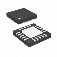
LTC6601CUF-2#TRPBF Linear Technology, LTC6601CUF-2#TRPBF Datasheet - Page 19

LTC6601CUF-2#TRPBF
Manufacturer Part Number
LTC6601CUF-2#TRPBF
Description
IC FILTER/ADC DVR LP LD 20-QFN
Manufacturer
Linear Technology
Datasheet
1.LTC6601CUF-2PBF.pdf
(40 pages)
Specifications of LTC6601CUF-2#TRPBF
Frequency - Cutoff Or Center
27MHz
Number Of Filters
3
Max-order
2nd
Voltage - Supply
2.7 V ~ 5.25 V
Mounting Type
Surface Mount
Package / Case
20-QFN
Lead Free Status / RoHS Status
Lead free / RoHS Compliant
Filter Type
-
Available stocks
Company
Part Number
Manufacturer
Quantity
Price
Part Number:
LTC6601CUF-2#TRPBFLTC6601CUF-2#PBF
Manufacturer:
Linear Technology
Quantity:
135
Likewise, substituting the numbers for a single 5V power
supply, (V
= 100Ω, into the above equation, the input common mode
range (V
The output common mode voltage is defi ned as the aver-
age of the two outputs:
The V
mode feedback loop which internally forces V
–V
1.1 V above V
middle of a voltage divider which sets the default mid-
supply open circuit potential.
In single supply applications, where the LTC6601 is used
to interface to an ADC, the optimal common mode input
to the ADC is often determined by the ADC’s reference. If
the ADC makes a reference available for setting the input
APPLICATIONS INFORMATION
Substituting the equation for Johnson noise of a resistor (e
e
e
no
no
0V ≤ V
OUT
V
=
=
OUTCM
OCM
–. The output common mode range extends from
⎛
⎝ ⎜
⎛
⎝ ⎜
INCMR
INCM
e
e
+
ni
ni
pin sets this average by an internal common
= V
= 5V, V
• 1+
• 1+
⎛
⎝ ⎜
⎛
⎝ ⎜
–
) is between the two limits:
≤ 4.7V
OCM
to 1V below V
R2
R2
–
R1
R1
=
= 0V) with V
⎞
⎠ ⎟
⎞
⎠ ⎟
V
⎞
⎠ ⎟
⎞
⎠ ⎟
OUT
2
2
+ 2 • I
+ 2 • I
+
+ V
2
+
⎛
⎜
⎜
⎝
⎛
⎜
⎜
⎝
. The V
OUT
n
n
OCM
2
2
• R2
• R2
–
⎛
⎜
⎝
⎛
⎜
⎝
= 2.5V, and R1 = R2
OCM
2
2
+ R3
+ R3
pin sits in the
2
2
• 1+
• 1+
OUT
⎛
⎝ ⎜
⎛
⎝ ⎜
+ =
R2
R2
R1
R1
⎞
⎠ ⎟
⎞
⎠ ⎟
2
2
⎞
⎟
⎠
nR
⎞
⎟
⎠
common mode voltage, it can be directly tied to the V
pin, but must be capable of driving the input impedance of
the V
to be connected to a mid-supply potential. If an external
reference drives the V
with a high quality 0.01μF or higher capacitor to a low
impedance ground plane to fi lter any thermal noise and
to prevent common mode signals on this pin from being
inadvertently converted to differential signals.
Noise Considerations
When comparing the LTC6601 noise to other amplifi ers,
be sure to compare similar specifi cations. Competing
devices often specify noise referred to the inputs of the
amplifi er. The input referred voltage noise of the LTC6601-2
is 4.7nV/√Hz.
In addition to the noise generated by the amplifi er, the
surrounding feedback resistors also contribute noise. A
noise model is shown in Figure 5. The output spot noise
generated by both the amplifi er and the feedback compo-
nents is governed by the equation:
⎞
⎟
⎟
⎠
⎞
⎟
⎟
⎠
= 4kTR), and simplifying:
+ 2 • e
+ 8 • k • T R2 1+
OCM
⎛
⎝ ⎜
nR1
pin (R
⎛
⎜
⎝
•
⎛
⎝ ⎜
R2
⎛
⎝ ⎜
R1
VOCM
⎞
⎠ ⎟
⎞
⎠ ⎟
R2
R1
). This impedance can be assumed
2
OCM
+ 2 e
⎞
⎠ ⎟
+ R3 1+
⎛
⎝ ⎜
pin, it should still be bypassed
nR3
⎛
⎝ ⎜
• 1+
⎛
⎝ ⎜
R2
R1
LTC6601-2
⎞
⎠ ⎟
R2
2
R1
⎞
⎟
⎠
⎞
⎠ ⎟
⎞
⎠ ⎟
2
+ 2 • e
19
nR2
66012f
OCM
2


