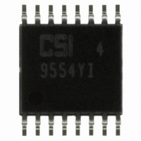
CAT9554YI-GT2 ON Semiconductor, CAT9554YI-GT2 Datasheet - Page 10

CAT9554YI-GT2
Manufacturer Part Number
CAT9554YI-GT2
Description
IC I/O EXPANDER I2C 8B 16TSSOP
Manufacturer
ON Semiconductor
Datasheet
1.CAT9554AWI-GT2.pdf
(16 pages)
Specifications of CAT9554YI-GT2
Interface
I²C, SMBus
Number Of I /o
8
Interrupt Output
Yes
Frequency - Clock
400kHz
Voltage - Supply
2.3 V ~ 5.5 V
Operating Temperature
-40°C ~ 85°C
Mounting Type
Surface Mount
Package / Case
16-TSSOP
Includes
POR
Lead Free Status / RoHS Status
Lead free / RoHS Compliant
Other names
9554YI-GT2
CAT9554YI-GT2TR
CAT9554YI-GT2TR
Available stocks
Company
Part Number
Manufacturer
Quantity
Price
Company:
Part Number:
CAT9554YI-GT2
Manufacturer:
ON
Quantity:
663
CAT9554, CAT9554A
The output port register sets the outgoing logic levels
of the I/O ports, defined as outputs by the
configuration register. Bit values in this register have
no effect on I/O pins defined as inputs. Reads from
the output port register reflect the value that is in the
flip-flop controlling the output, not the actual I/O
pin value.
The polarity inversion register allows the user to invert
the polarity of the input port register data. If a bit in
this register is set (“1”) the corresponding input port
data is inverted. If a bit in the polarity inversion
register is cleared (“0”), the original input port polarity
is retained.
The configuration register sets the directions of the
ports. Set the bit in the configuration register to enable
FROM PO RT
Doc. No. MD-9002 Rev. F
WRITE TO
REGISTER
WRITE TO
DATA OUT
SDA
SCL
PORT
SDA
SCL
start condition
start condition
S
S
1
1
0
0
2
2
1
1
slave address
slave address
3
3
0
0
4
4
Figure 10. Write to Configuration or Polarity Inversion Register
0
0
A2
A2
5
5
acknowledge
acknowledge
A1
A1
6
6
from slave
from slave
A0
A0
7
7
R/W
R/W
0
Figure 9. Write to Output Port Register
8
0
8
9
A
9
A
0
0
0
0
command byte
0
acknowledge from slave
command byte
0
acknowledge from slave
0
0
10
0
0
the corresponding port pin as an input with a high
impedance output driver. If a bit in this register is
cleared, the corresponding port pin is enabled as an
output. At power-up, the I/Os are configured as inputs
with a weak pull-up resistor to V
Data is transmitted to the CAT9554/9554A registers
using the write mode shown in Figure 9 and Figure 10.
The CAT9554/9554A registers are read according to
the timing diagrams shown in Figure 11 and Figure
12. Once a command byte has been sent, the register
which was addressed will continue to be accessed by
reads until a new command byte will be sent.
0
0
0
1 1/0
1
A
A
acknowledge from slave
data to port
data to register
DATA 1
acknowledge from slave
Characteristics subject to change without notice
DATA 1
CC
© 2008 SCILLC. All rights reserved
.
t pv
A
stop
condition
DATA 1 VALID
P
A
stop
condition
P


