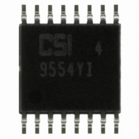
CAT9554YI-GT2 ON Semiconductor, CAT9554YI-GT2 Datasheet - Page 9

CAT9554YI-GT2
Manufacturer Part Number
CAT9554YI-GT2
Description
IC I/O EXPANDER I2C 8B 16TSSOP
Manufacturer
ON Semiconductor
Datasheet
1.CAT9554AWI-GT2.pdf
(16 pages)
Specifications of CAT9554YI-GT2
Interface
I²C, SMBus
Number Of I /o
8
Interrupt Output
Yes
Frequency - Clock
400kHz
Voltage - Supply
2.3 V ~ 5.5 V
Operating Temperature
-40°C ~ 85°C
Mounting Type
Surface Mount
Package / Case
16-TSSOP
Includes
POR
Lead Free Status / RoHS Status
Lead free / RoHS Compliant
Other names
9554YI-GT2
CAT9554YI-GT2TR
CAT9554YI-GT2TR
Available stocks
Company
Part Number
Manufacturer
Quantity
Price
Company:
Part Number:
CAT9554YI-GT2
Manufacturer:
ON
Quantity:
663
CAT9554, CAT9554A
ACKNOWLEDGE
After a successful data transfer, each receiving device
is required to generate an acknowledge. The
acknowledging device pulls down the SDA line during
the ninth clock cycle, signaling that it received the 8
bits of data. The SDA line remains stable LOW during
the HIGH period of the acknowledge related clock
pulse (Figure 5).
The CAT9554/9554A respond with an acknowledge
after receiving a START condition and its slave
address. If the device has been selected along with a
write operation, it responds with an acknowledge after
receiving each 8-bit byte.
When the CAT9554/9554A begins a READ mode it
transmits 8 bits of data, releases the SDA line, and
monitors the line for an acknowledge. Once it receives
this acknowledge, the CAT9554/9554A will continue
to transmit data. If no acknowledge is sent by the
Master, the device terminates data transmission and
waits for a STOP condition. The master must then
issue a STOP condition to return the CAT9554/9554A
to the standby power mode and place the device in a
known state.
REGISTERS AND BUS TRANSACTIONS
The CAT9554/9554A consist of an input port register,
an output port register, a polarity inversion register
and a configuration register. Table 1 shows the
register address table. Tables 2 to 5 list Register 0
through Register 3 information.
Table 1. Register Command Byte
© 2008 SCILLC. All rights reserved
Characteristics subject to change without notice
Command
(hex)
0x00
0x01
0x02
0x03
FROM TRANSMITTER
FROM RECEIVER
DATA OUTPUT
DATA OUTPUT
SCL FROM
Read/write byte
Read/write byte
Read/write byte
MASTER
Read byte
Protocol
START
BUS RELEASE DELAY (TRANSMITTER)
Polarity inversion register
Configuration register
Output port register
Input port register
1
Function
Figure 8. Acknowledge Timing
ACK DELAY
9
The command byte is the first byte to follow the device
address byte during a write/read bus transaction. The
register command byte acts as a pointer to determine
which register will be written or read.
The input port register is a read only port. It reflects
the incoming logic levels of the I/O pins, regardless of
whether the pin is defined as an input or an output by
the configuration register. Writes to the input port
register are ignored.
Table 2. Register 0 – Input Port Register
Table 3. Register 1 – Output Port Register
Table 4. Register 2 – Polarity Inversion Register
Table 5. Register 3 – Configuration Register
8
default
default
default
default
bit
bit
bit
bit
O
N
C
I
1
1
0
1
7
7
7
7
9
ACK SETUP
O
N
C
I
1
1
0
1
6
6
6
6
O
N
C
BUS RELEASE DELAY (RECEIVER)
I
1
1
0
1
5
5
5
5
O
N
C
I
1
1
0
1
4
4
4
4
O
N
C
I
1
0
1
1
3
3
3
3
O
C
N
1
Doc. No. MD-9002, Rev. F
I
1
0
1
2
2
2
2
O
N
C
I
1
1
0
1
1
1
1
1
O
N
C
I
1
1
0
1
0
0
0
0


