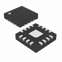
MAX7316ATE+ Maxim Integrated Products, MAX7316ATE+ Datasheet - Page 2

MAX7316ATE+
Manufacturer Part Number
MAX7316ATE+
Description
IC I/O EXPANDER I2C 16B 16TQFN
Manufacturer
Maxim Integrated Products
Datasheet
1.MAX7316AEE.pdf
(24 pages)
Specifications of MAX7316ATE+
Interface
I²C, SMBus
Number Of I /o
10
Interrupt Output
Yes
Frequency - Clock
400kHz
Voltage - Supply
2 V ~ 3.6 V
Operating Temperature
-40°C ~ 125°C
Mounting Type
Surface Mount
Package / Case
16-TQFN Exposed Pad
Lead Free Status / RoHS Status
Lead free / RoHS Compliant
ABSOLUTE MAXIMUM RATINGS
Voltage (with respect to GND)
V+ .............................................................................-0.3V to +4V
SCL, SDA, AD0, BLINK, RST, P0–P7 .......................-0.3V to +6V
INT/O8 ......................................................................-0.3V to +8V
DC Current on P0–P7, INT/O8 ............................................55mA
DC Current on SDA.............................................................10mA
Maximum GND Current ....................................................190mA
ELECTRICAL CHARACTERISTICS
(Typical Operating Circuit, V+ = 2V to 3.6V, T
(Note 1)
10-Port I/O Expander with LED Intensity
Control, Interrupt, and Hot-Insertion Protection
Stresses beyond those listed under “Absolute Maximum Ratings” may cause permanent damage to the device. These are stress ratings only, and functional
operation of the device at these or any other conditions beyond those indicated in the operational sections of the specifications is not implied. Exposure to
absolute maximum rating conditions for extended periods may affect device reliability.
2
Operating Supply Voltage
Output Load External Supply
Voltage
Standby Current
(Interface Idle, PWM Disabled)
Supply Current
(Interface Idle, PWM Enabled)
Supply Current
(Interface Running, PWM
Disabled)
Supply Current
(Interface Running, PWM
Enabled)
Input High Voltage
SDA, SCL, AD0, BLINK, P0–P7
Input Low Voltage
SDA, SCL, AD0, BLINK, P0–P7
Input Leakage Current
SDA, SCL, AD0, BLINK, P0–P7
Input Capacitance
SDA, SCL, AD0, BLINK, P0–P7
_______________________________________________________________________________________
PARAMETER
SYMBOL
I
V
IH
V
V+
V
EXT
I
I
I
I
, I
+
+
+
+
IH
IL
IL
A
S C L and S D A at V + ; other
d i g i tal i np uts at V + or GN D ;
P WM i ntensi ty contr ol d i sab l ed
S C L and S D A at V + ; other
d i g i tal i np uts at V + or GN D ;
P WM i ntensi ty contr ol enab l ed
f
inputs at V+ or GND; PWM
intensity control disabled
f
inputs at V+ or GND; PWM
intensity control enabled
Input = GND or V+
SCL
SCL
= T
MIN
= 400kHz; other digital
= 400kHz; other digital
to T
MAX
, unless otherwise noted. Typical values are at V+ = 3.3V, T
CONDITIONS
Continuous Power Dissipation (T
Operating Temperature Range (T MIN to T MAX )-40°C to +125°C
Junction Temperature ......................................................+150°C
Storage Temperature Range .............................-65°C to +150°C
Lead Temperature (soldering, 10s) .................................+300°C
16-Pin QSOP (derate 8.3mW/°C over +70°C)..............667mW
16-Pin QFN (derate 14.7mW/°C over +70°C) ............1177mW
T
T
T
T
T
T
T
T
T
T
T
T
A
A
A
A
A
A
A
A
A
A
A
A
= +25°C
= -40°C to +85°C
= T
= +25°C
= -40°C to +85°C
= T
= +25°C
= -40°C to +85°C
= T
= +25°C
= -40°C to +85°C
= T
MIN
MIN
MIN
MIN
to T
to T
to T
to T
MAX
MAX
MAX
MAX
0.7 x
MIN
-0.2
2.0
V+
A
0
= +70°C)
TYP
1.2
40
51
7
8
MAX
0.3 x
+0.2
12.1
13.3
14.4
110
117
122
3.6
5.5
2.3
2.6
3.3
V+
76
78
80
A
= +25°C.)
UNITS
µA
µA
µA
µA
µA
pF
V
V
V
V


