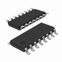
SI3056-D-FS Silicon Laboratories Inc, SI3056-D-FS Datasheet - Page 30

SI3056-D-FS
Manufacturer Part Number
SI3056-D-FS
Description
IC ISOMODEM SYSTEM-SIDE 16SOIC
Manufacturer
Silicon Laboratories Inc
Type
Chipsetr
Datasheet
1.SI3056-D-FS.pdf
(94 pages)
Specifications of SI3056-D-FS
Package / Case
16-SOIC (3.9mm Width)
Data Format
V.92
Interface
Serial
Voltage - Supply
3 V ~ 3.6 V
Mounting Type
Surface Mount
Product
Modem Module
Supply Voltage (min)
3 V
Supply Current
15 mA
Maximum Operating Temperature
+ 70 C
Minimum Operating Temperature
0 C
Mounting Style
SMD/SMT
Lead Free Status / RoHS Status
Lead free / RoHS Compliant
Baud Rates
-
Lead Free Status / RoHS Status
Lead free / RoHS Compliant, Lead free / RoHS Compliant
Available stocks
Company
Part Number
Manufacturer
Quantity
Price
Company:
Part Number:
SI3056-D-FS
Manufacturer:
FAIRCHILD
Quantity:
130
Company:
Part Number:
SI3056-D-FSR
Manufacturer:
DSC
Quantity:
1 200
Si3018/19/10
while the RNG1-RNG2 voltage is between the
thresholds. When the ring becomes positive, DTX
transitions to +32767. When the ring signal goes near 0,
DTX remains near 1228. As the ring becomes negative,
the DTX transitions to –32768. This repeats in cadence
with the ring signal.
To observe the ring signal on DTX, watch the MSB of
the data. The MSB toggles at the same frequency as
the ring signal independent of the ring detector mode.
This method is adequate for determining the ring
frequency.
5.15. Ring Validation
This feature prevents false triggering of a ring detection
by validating the ring frequency. Invalid signals, such as
a line voltage change when a parallel handset goes off-
hook, pulse dialing, or a high-voltage line test are
ignored. Ring validation can be enabled during normal
operation and in low power sleep mode. The external
MCLK signal is required in low power sleep mode for
ring validation.
The ring validation circuit operates by calculating the
time between alternating crossings of positive and
negative ring thresholds to validate that the ring
frequency is within tolerance. High and low frequency
tolerances are programmable in the RAS[5:0] and
RMX[5:0] fields. The RCC[2:0] bits define how long the
ring signal must be within tolerance.
Once the duration of the ring frequency is validated by
the RCC bits, the circuitry stops checking for frequency
tolerance and begins checking for the end of the ring
signal, which is defined by a lack of additional threshold
crossings for a period of time configured by the
RTO[3:0] bits. When the ring frequency is first validated,
a timer defined by the RDLY[2:0] bits is started. If the
RDLY[2:0] timer expires before the ring timeout, then
the ring is validated and a valid ring is indicated. If the
ring timeout expires before the RDLY[2:0] timer, a valid
ring is not indicated.
Ring validation requires five parameters:
30
Timeout parameter to place a lower limit on the
frequency of the ring signal on the RAS[5:0] bits
(Register 24). This is measured by calculating the
time between crossings of positive and negative ring
thresholds.
Minimum count to place an upper limit on the
frequency on the RMX[5:0] bits (Register 22).
Time interval over which the ring signal must be the
correct frequency on the RCC[2:0] bits (Register 23).
Timeout period that defines when the ring pulse has
ended based on the most recent ring threshold
crossing.
Rev. 1.05
The RNGV bit (Register 24, bit 7) enables or disables
the ring validation feature in normal operating mode and
low-power sleep mode.
Ring validation affects the behavior of the RDT status
bit, the RDTI interrupt, the INT pin, and the RGDT pin.
1. When ring validation is enabled, the status bit seen
2. The RDTI interrupt fires when a validated ring
3. The INT pin follows the RDTI bit with configurable
The RGDT pin can be configured to follow the ringing
signal envelope detected by the ring validation circuit by
setting RFWE to 0. If RFWE is set to 1, the RGDT pin
follows an unqualified ring detect one-shot signal
initiated by a ring-threshold crossing and terminated by
a fixed counter timeout of approximately 5 seconds.
(This information is shown in Register 18).
5.16. Ringer Impedance and Threshold
The ring detector in many DAAs is ac coupled to the line
with a large 1 µF, 250 V decoupling capacitor. The ring
detector on the Si3056 is resistively coupled to the line.
This produces a high ringer impedance to the line of
approximately 20 M Ω to meet the majority of country
PTT specifications, including FCC and TBR21.
Several countries including Poland, and South Africa,
may require a maximum ringer impedance that can be
met with an internally synthesized impedance by setting
the RZ bit (Register 16, bit 1).
Some
differently. The RT bit (Register 16, bit 0) selects
between two different ringer thresholds: 15 V ±10% and
21.5 V ±10%. These two settings satisfy ringer
threshold requirements worldwide. The thresholds are
set so that a ring signal is guaranteed to not be detected
below the minimum, and a ring signal is guaranteed to
be detected above the maximum.
Delay period between when the ring signal is
validated and when a valid ring signal is indicated to
accommodate distinctive ringing.
in the RDT read-only bit (r5.2), represents the
detected envelope of the ring. The ring validation
parameters are configurable so that this envelope
may remain high throughout a distinctive-ring
sequence.
occurs. If RDI is zero (default), the interrupt occurs
on the rising edge of RDT. If RDI is set, the interrupt
occurs on both rising and falling edges of RDT.
polarity.
countries
also
specify
ringer
thresholds


