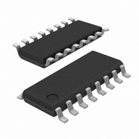
SI3012-KS Silicon Laboratories Inc, SI3012-KS Datasheet - Page 29

SI3012-KS
Manufacturer Part Number
SI3012-KS
Description
IC ISOMODEM SYSTEM-SIDE 16SOIC
Manufacturer
Silicon Laboratories Inc
Datasheet
1.SI3012-KS.pdf
(64 pages)
Specifications of SI3012-KS
Data Format
V.90
Interface
Serial
Voltage - Supply
3.3 V ~ 5 V
Mounting Type
Surface Mount
Package / Case
16-SOIC (3.9mm Width)
Lead Free Status / RoHS Status
Contains lead / RoHS non-compliant
Baud Rates
-
Lead Free Status / RoHS Status
Lead free / RoHS Compliant, Contains lead / RoHS non-compliant
Available stocks
Company
Part Number
Manufacturer
Quantity
Price
Company:
Part Number:
SI3012-KS
Manufacturer:
SILICON/60
Quantity:
950
Part Number:
SI3012-KS
Manufacturer:
SILICON LABS/芯科
Quantity:
20 000
Part Number:
SI3012-KSR
Manufacturer:
SI
Quantity:
20 000
near a transition level. The LCS value is a rough
approximation of the loop current, and the designer is
advised to use this value in a relative means rather than
an absolute value.
This feature enables the modem to determine if an
additional line has “picked up” while the modem is
transferring information. In the case of a second phone
going off-hook, the loop current falls approximately 50%
and is reflected in the value of the LCS bits.
Overload Detection
The Si3038 can detect if an overload condition is
present which may damage the DAA circuit. The DAA
may be damaged if excessive line voltage or loop
current is sustained.
In FCC and Japan dc termination modes, an LCS[3:0]
value of 1111b means the loop current is greater than
120 mA indicating the DAA is drawing excessive loop
current.
In CTR21 mode, 120 mA of loop current is not possible
due to the current limit circuit. In this dc termination
mode, an LCS[3:0] value of 1000b (8 decimal) or
greater indicates an excessive loop current condition.
Analog Output
The Si3038 supports an analog output (AOUT) for
driving the call progress speaker. AOUT is an analog
signal comprised of a mix of the transmit and receive
signals.
The AOUT level can be adjusted via the ATM and ARM
bits in control register 5Ch. The transmit portion of
AOUT can be set to –20 dB, –26 dB, –32 dB, or mute.
The receive portion of AOUT can be set to 0 dB, –6 dB,
–12 dB, or mute. Figure 20 on page 19 illustrates a
recommended application circuit. Note that in the
configuration shown, the LM386 provides a gain of 26
dB. Additional gain adjustments may be made by
varying the voltage divider created by R1 and R3.
Gain Control
The Si3038 supports multiple gain and attenuation
settings in register 46h/48h for the receive and transmit
paths, respectively. The receive path can support gains
of 0, 3, 6, 9, and 12 dB, as selected by ADC[3:1] bits.
The receive path can also be muted by setting bit 7. The
transmit path can support attenuations of 0, 3, 6, 9, and
12 dB, as selected by DAC[3:1] bits. The transmit path
can also be muted by setting bit 15.
Filter Selection
The Si3038 supports additional filter selections for the
receive and transmit signals. The IIRE bit of register
5Ch, when set, enables the IIR filters. This filter
Rev. 2.01
provides a much lower, however non-linear, group delay
than the default FIR filters.
In-Circuit Testing
The Si3038’s advanced design provides the modem
manufacturer with increased ability to determine system
functionality during production line tests, as well as user
diagnostics. Several loopback modes exist allowing
increased coverage of system components.
The loopback mode allows the data pump to provide a
digital input test pattern on SDATA_IN and receive a
corresponding digital test pattern back on SDATA_OUT.
To enable this mode, set L1B[2:0](L2B[2:0])=101 in
register 56h. In this mode, the isolation barrier is
actually being tested. The digital stream is delivered
across the isolation capacitors, C1 and C2 of Figure 19
on page 16, to the line-side device and returned across
the same barrier.
The digital DAC loopback mode allows data to be sent
on the digital path from SDATA_IN to the digital section
of DAC to ADC to SDATA_OUT. This loopback mode is
used when the line-side chip is in power-down mode. To
enable this mode, set L1B[2:0](L2B[2:0]) = 011 in
register 56h.
The remote analog loopback mode allows an external
device to drive the receive pins of the line-side chip and
receive the signal from the transmit pins. This mode
allows testing of external components connecting the
RJ-11 jack (TIP and RING) to the line side of the
Si3014. To enable this mode, set L1B2:0(L2B2:0) = 100
in register 56h.
The ADC loopback mode allows an external device to
drive the receive pins of the Si3014. The signal is then
digitized on the Si3014 and sent to the Si3024, which
sends the data back to the Si3014. The signal is then
converted back to analog. The external device receives
the signal on the transmit pins. This mode allows testing
of the Si3038s converters and external devices between
the Si3014 and RJ-11 jack. To enable this mode, set the
L1B[2:0](L2B[2:0]) = 001.
The final two testing modes, local analog loopback and
external analog loopback, allow the system to test the
basic operation of the converters on the line side and
the functionality of the external components. In local
analog loopback mode, the AC’97 controller provides a
digital test waveform on SDATA_OUT. This data is
passed across the isolation barrier, converted to analog,
internally looped to the receive path, converted to
digital, passed back across the isolation barrier, and
presented to the AC’97 controller. To enable local and
analog loopback, set L1B2:0 (L2B2:0) = 010. External
analog loopback mode allows the system to test
external components by passing converted data (from
Si3038
29


