AD698APZ Analog Devices Inc, AD698APZ Datasheet
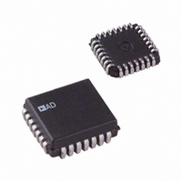
IC LVDT SIGNAL COND 28-PLCC

AD698APZ

Manufacturer Part Number
AD698APZ
Description
IC LVDT SIGNAL COND 28-PLCC
Manufacturer
Analog Devices Inc
Type
Signal Conditionerr
Datasheet

Specifications of AD698APZ

Input Type
Voltage
Output Type
Voltage
Interface
LVDT
Current - Supply
15mA
Mounting Type
Surface Mount
Package / Case
28-LCC (J-Lead)
Bandwidth
20kHz
Supply Voltage Min
13V
Supply Voltage Max
36V
Digital Ic Case Style
LCC
No. Of Pins
28
Operating Temperature Range
-40°C To +85°C
Msl
MSL 5 - 48 Hours
Supply Voltage Range
13V To 36V
Audio Ic Case Style
PLCC
Base Number
698
Rohs Compliant
Yes
Lead Free Status / RoHS Status
Lead free / RoHS Compliant
Lead Free Status / RoHS Status
Lead free / RoHS Compliant, Lead free / RoHS Compliant

Available stocks

Company
Part Number
Manufacturer
Quantity
Price
Part Number:
AD698APZ
Manufacturer:
Analog Devices Inc
Quantity:
135
Part Number:
AD698APZ
Manufacturer:
ADI
Quantity:
3 271
Part Number:
AD698APZ
Manufacturer:
Analog Devices Inc
Quantity:
10 000
Part Number:
AD698APZ
Manufacturer:
ADI/亚德诺
Quantity:
20 000
Part Number:
AD698APZ / ROHS
Quantity:
1 400
a
PRODUCT DESCRIPTION
The AD698 is a complete, monolithic Linear Variable Differen-
tial Transformer (LVDT) signal conditioning subsystem. It is
used in conjunction with LVDTs to convert transducer mechan-
ical position to a unipolar or bipolar dc voltage with a high de-
gree of accuracy and repeatability. All circuit functions are
included on the chip. With the addition of a few external passive
components to set frequency and gain, the AD698 converts the
raw LVDT output to a scaled dc signal. The device will operate
with half-bridge LVDTs, LVDTs connected in the series op-
posed configuration (4-wire), and RVDTs.
The AD698 contains a low distortion sine wave oscillator to
drive the LVDT primary. Two synchronous demodulation
channels of the AD698 are used to detect primary and second-
ary amplitude. The part divides the output of the secondary by
the amplitude of the primary and multiplies by a scale factor.
This eliminates scale factor errors due to drift in the amplitude
of the primary drive, improving temperature performance and
stability.
The AD698 uses a unique ratiometric architecture to eliminate
several of the disadvantages associated with traditional ap-
proaches to LVDT interfacing. The benefits of this new cir-
cuit are: no adjustments are necessary; temperature stability is
improved; and transducer interchangeability is improved.
The AD698 is available in two performance grades:
Grade
AD698AP
AD698SQ
REV. B
Information furnished by Analog Devices is believed to be accurate and
reliable. However, no responsibility is assumed by Analog Devices for its
use, nor for any infringements of patents or other rights of third parties
which may result from its use. No license is granted by implication or
otherwise under any patent or patent rights of Analog Devices.
FEATURES
Single Chip Solution, Contains Internal Oscillator and
No Adjustments Required
Interfaces to Half-Bridge, 4-Wire LVDT
DC Output Proportional to Position
20 Hz to 20 kHz Frequency Range
Unipolar or Bipolar Output
Will Also Decode AC Bridge Signals
Outstanding Performance
Voltage Reference
Linearity: 0.05%
Output Voltage:
Gain Drift: 20 ppm/ C (typ)
Offset Drift: 5 ppm/ C (typ)
Temperature Range
–40 C to +85 C
–55 C to +125 C
11 V
Package
28-Pin PLCC
24-Pin Cerdip
PRODUCT HIGHLIGHTS
1. The AD698 offers a single chip solution to LVDT signal
2. The AD698 can be used with many different types of posi-
3. The 20 Hz to 20 kHz excitation frequency is determined by a
4. Changes in oscillator amplitude with temperature will not af-
5. Multiple LVDTs can be driven by a single AD698 either in
6. The AD698 may be used as a loop integrator in the design of
7. The sum of the transducer secondary voltages do not need to
One Technology Way, P.O. Box 9106, Norwood. MA 02062-9106, U.S.A.
Tel: 617/329-4700
conditioning problems. All active circuits are on the mono-
lithic chip with only passive components required to com-
plete the conversion from mechanical position to dc voltage.
tion sensors. The circuit is optimized for use with any
LVDT, including half-bridge and series opposed, (4 wire)
configurations. The AD698 accommodates a wide range of
input and output voltages and frequencies.
single external capacitor. The AD698 provides up to 24 volts
rms to differentially drive the LVDT primary, and the
AD698 meets its specifications with input levels as low as
100 millivolts rms.
fect overall circuit performance. The AD698 computes the
ratio of the secondary voltage to the primary voltage to deter-
mine position and direction. No adjustments are required.
series or parallel as long as power dissipation limits are not
exceeded. The excitation output is thermally protected.
simple electromechanical servo loops.
be constant.
FUNCTIONAL BLOCK DIAGRAM
LVDT Signal Conditioner
B
A
AMP
OSCILLATOR
A
B
© Analog Devices, Inc., 1995
FILTER
AD698
REFERENCE
Universal
VOLTAGE
AD698
Fax: 617/326-8703
AMP

Related parts for AD698APZ

AD698APZ Summary of contents

Page 1

FEATURES Single Chip Solution, Contains Internal Oscillator and Voltage Reference No Adjustments Required Interfaces to Half-Bridge, 4-Wire LVDT DC Output Proportional to Position kHz Frequency Range Unipolar or Bipolar Output Will Also Decode AC Bridge ...

Page 2

AD698–SPECIFICATIONS Parameter 1 TRANSFER FUNCTION OVERALL ERROR MIN MAX SIGNAL OUTPUT CHARACTERISTICS Output Voltage Range Output Current MIN MAX Short Circuit Current 2 Nonlinearity MIN MAX 3 Gain Error Gain Drift ...

Page 3

NOTES 1 A and B represent the Mean Average Deviation (MAD) of the detected sine waves V multiply V +1 for A > and V OUT COMP+ COMP– OUT 2 Nonlinearity of the AD698 only in units of ...

Page 4

AD698 Typical Characteristics (at +25 C and V 240 200 160 GAIN PSRR 15–18V 120 80 40 GAIN PSRR 12–15V 20 OFFSET PSRR 12–15V 0 OFFSET PSRR 15–18V –20 –60 –40 – TEMPERATURE – C Figure ...

Page 5

THEORY OF OPERATION A block diagram of the AD698 along with an LVDT (linear variable differential transformer) connected to its input is shown in Figure 5 below. The LVDT is an electromechanical trans- ducer—its input is the mechanical displacement of ...

Page 6

AD698 CONNECTING THE AD698 The AD698 can easily be connected for dual or single supply operation as shown in Figures 7, 8 and 13. The following gen- eral design procedures demonstrate how external component values are selected and can be ...

Page 7

Multiply the primary excitation voltage by the VTR to get the expected secondary voltage at mechanical full scale. For example, for an LVDT with a sensitivity of 2.4 mV/V/mil and a full scale of 0.1 inch, the VTR = 0.0024 ...

Page 8

AD698 Note that V should be chosen so that R3 cannot have negative OS value . Figure 12 shows the desired response. V (VOLTS) OUT +10 +5 +0.1d (INCHES) –0.1 Figure 12 V–10 V Full Scale) vs. Displacement ...

Page 9

R2 = 81k – 10kHz EXC –70 0 0.033µF –60 –120 –180 0.1µF –240 R2 = 81k –300 f = 10kHz EXC –360 –420 0 100 1k FREQUENCY – Hz ...

Page 10

AD698 Determining LVDT Sensitivity LVDT sensitivity can be determined by measuring the LVDT secondary voltages as a function of primary drive and core posi- tion, and performing a simple computation. Energize the LVDT at its recommended primary drive level, V ...

Page 11

OUT Solving for 400 and setting R OUT [400 – 19. Choose an oscillator amplitude that is in the range ...

Page 12

AD698 0.005 (0.13) MIN PIN 1 0.200 (5.08) MAX 0.200 (5.08) 0.125 (3.18) 0.023 (0.58) 0.014 (0.36) 0.048 (1.21) 0.042 (1.07) OUTLINE DIMENSIONS Dimensions shown in inches and (mm). 24-Pin Cerdip (Wide) 0.098 (2.49) MAX 24 13 0.610 (15.5) 0.520 ...

Related keywords