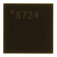
SX8724E082TRT Semtech, SX8724E082TRT Datasheet - Page 7

SX8724E082TRT
Manufacturer Part Number
SX8724E082TRT
Description
IC DAS PRESSURE/TEMP SENS 16MLPQ
Manufacturer
Semtech
Series
ZoomingADC™r
Type
Pressure/Temperature Sensorr
Datasheet
1.SX8724E082TRT.pdf
(53 pages)
Specifications of SX8724E082TRT
Input Type
Differential
Output Type
Digital
Interface
2-Wire
Mounting Type
Surface Mount
Package / Case
16-MLPQ
For Use With
XE8000EV121 - BOARD EVAL FOR SX8723/24
Lead Free Status / RoHS Status
Lead free / RoHS Compliant
Current - Supply
-
Other names
SX8724E082TR
ADVANCED COMMUNICATIONS & SENSING
Notes:
(1)
(2)
(3)
(4)
(5)
(6)
(7)
(8)
(9)
(10) Offset error is defined as the output code error for a zero volt input (ideally, output code = 0). For
(11) INL defined as the deviation of the DC transfer curve of each individual code from the best-fit straight line. This specification holds
(12) DNL is defined as the difference (in LSB) between the ideal (1 LSB) and measured code transitions for successive codes.
(13) Figures for Gains = 1 to 100. PSRR is defined as the amount of change in the ADC output value as the power supply voltage
(14) Conversion time is given by: T
(15) PGAs are reset after each writing operation to registers RegACCfg1-5. The ADC must be started after a PGA or inputs common-
(16) Nominal (maximum) bias currents in PGAs and ADC, i.e. IB_AMP_PGA[1:0] = '11' and IB_AMP_ADC[1:0] = '11'.
(17) Bias currents in PGAs and ADC set to 3/4 of nominal values, i.e. IB_AMP_PGA[1:0] = '10', IB_AMP_ADC[1:0] = '10'.
(18) Bias currents in PGAs and ADC set to 1/2 of nominal values, i.e. IB_AMP_PGA[1:0] = '01', IB_AMP_ADC[1:0] = '01'.
(19) Bias currents in PGAs and ADC set to 1/4 of nominal values, i.e. IB_AMP_PGA[1:0] = '00', IB_AMP_ADC[1:0] = '00'.
V1.23 © 2009 Semtech Corp.
Nbr of End Conversion Cycles
PGA Stabilization Delay
ADC Digital Output
Output Data Coding
Power Supply
Voltage Supply Range
Analog Quiescent Current
Total Consumption
ADC Only Consumption
PGA1 Consumption
PGA2 Consumption
PGA3 Consumption
Analog Power Dissipation
Normal Power Mode
3/4 Power Reduction Mode
1/2 Power Reduction Mode
1/4 Power Reduction Mode
Temperature
Operating Range
Gain
V
Offset due to tolerance on GDoff
Measured with block connected to inputs through AMUX block. Normalized input sampling frequency for input impedance is f
500kHz. This figure must be multiplied by 2 for f
Figure independent on PGA1 gain and sampling frequency f
Figure independent on PGA2 gain and sampling frequency f
Figure independent on PGA3 gain and sampling frequency f
Resolution is given by n = 2 log2(OSR) + log2(N
2, 4 or 8.
If a ramp signal is applied to the input, all digital codes appear in the resulting ADC output data.
Gain error is defined as the amount of deviation between the ideal (theoretical) transfer function and the measured transfer function
(with the offset error removed).
over the full scale. (For 16 bits INL set PGA3 on).
changes.
be set to 1, 2, 4 or 8.
mode stabilization delay. This is done by writing bit Start several cycles after PGA settings modification or channel switching. Delay
between PGA start or input channel switching and ADC start should be equivalent to OSR (between 8 and 1024) number of cycles.
This delay does not apply to conversions made without the PGAs.
IN, MAX
= (V
Parameter
defined
REF,ADC
/2) (OSR/OSR+1).
as
overall
CONV
2
or GDoff
PGA
= (N
N
V
I
Symbol
Q
DD
END
ELCONV
3
gain
setting. For small intrinsic offset, use only ADC and PGA1.
ZoomingADC™ for Pressure and Temperature Sensing
S
(OSR + 1) + 1) / f
ELCONV
= 250kHz, 4 for f
(Note 15)
Binary Two’s Complement
See Table 15 and Table 16
Only ZoomingADC
V
V
V
V
V
All PGAs & ADC Active
V
V
V
V
DD
DD
DD
DD
DD
DD
DD
DD
DD
GD
Comments / Conditions
= 5V/3V
= 5V/3V
= 5V/3V
= 5V/3V
= 5V/3V
= 5V/3V (Note 16)
= 5V/3V (Note 17)
= 5V/3V (Note 18)
= 5V/3V (Note 19)
). OSR can be set between 8 and 1024, in powers of 2. N
TOT
S
S
S
.
.
.
=
7
S
S
GD
. OSR can be set between 8 and 1024, in powers of 2. N
= 125kHz. Input impedance is proportional to 1/ f
1
GD
2
GD
3
.
Maximum
Min
-40
2.4
0
input
800/675
260/190
190/170
150/135
200/180
4.0/2.0
3.2/1.6
2.4/1.1
1.5/0.7
1 LSB offset, N
OSR
Typ
5
voltage
www.semtech.com
ELCONV
Max
125
5.5
ELCONV
5
S
is
.
can be set to 1,
SX8724
must be 2.
given
ELCONV
cycles
cycles
Unit
mW
mW
mW
mW
° C
V
A
A
A
A
A
can
S
by:
=


