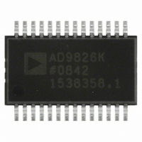
AD9826KRSZ Analog Devices Inc, AD9826KRSZ Datasheet - Page 14

AD9826KRSZ
Manufacturer Part Number
AD9826KRSZ
Description
IC IMAGE SGNL PROC 16BIT 28-SSOP
Manufacturer
Analog Devices Inc
Type
Image Sensorr
Datasheet
1.AD9826KRSZRL.pdf
(20 pages)
Specifications of AD9826KRSZ
Input Type
Logic
Output Type
Logic
Interface
3-Wire Serial
Current - Supply
75mA
Mounting Type
Surface Mount
Package / Case
28-SSOP
Ic Interface Type
Serial
Supply Voltage Range
4.75V To 5.25V, 3V To 5.25V
Power Dissipation Pd
400mW
Operating Temperature Range
-40°C To +85°C
Digital Ic Case Style
SSOP
No. Of Pins
28
Lead Free Status / RoHS Status
Lead free / RoHS Compliant
Available stocks
Company
Part Number
Manufacturer
Quantity
Price
Company:
Part Number:
AD9826KRSZ
Manufacturer:
AD
Quantity:
5 510
Part Number:
AD9826KRSZ
Manufacturer:
ADI/亚德诺
Quantity:
20 000
Part Number:
AD9826KRSZ-REEL
Manufacturer:
ADI/亚德诺
Quantity:
20 000
Company:
Part Number:
AD9826KRSZRL
Manufacturer:
ST
Quantity:
2 904
Part Number:
AD9826KRSZRL
Manufacturer:
ADI/亚德诺
Quantity:
20 000
AD9826
adjust pin. A voltage applied to this pin will be subtracted from
the voltages applied to the Red, Green, and Blue inputs in the first
amplifier stage of the AD9826. The input clamp is disabled in this
mode. For more information, see the Circuit Operation section.
Timing for this mode is shown in Figure 4. CDSCLK1 should
be grounded in this mode. The rising edge of CDSCLK2 should
not occur before the previous falling edge of ADCCLK, as shown
by t
offset and gain values for the Red, Green, and Blue channels are
programmed using the serial interface. The order in which the
channels are switched through the multiplexer is selected by
programming the MUX Configuration Register.
1-Channel CDS Mode
This mode operates the same way as the 3-Channel CDS mode.
The difference is that the multiplexer remains fixed in this mode,
so only the channel specified in the MUX Configuration Regis-
ter is processed.
Timing for this mode is shown in Figure 2.
1-Channel SHA Mode
This mode operates the same way as 3-Channel SHA mode,
except that the multiplexer remains stationary. Only the channel
specified in the MUX Configuration Register is processed.
Timing for this mode is shown in Figure 6. CDSCLK1 should
be grounded in this mode of operation.
Configuration Register
The Configuration Register controls the AD9826’s operating
mode and bias levels. Bits D8 and D1 should always be set low.
D
Set
to
0
Register
Name
Configuration
MUX Config
Red PGA
Green PGA
Blue PGA
Red Offset
Green Offset
Blue Offset
Power-on default value.
8
ADC2
D7
Input Range Internal VREF 3CH Mode
1 = 4 V
0 = 2 V
. The output data latency is three ADCCLK cycles. The
A2 A1 A0
0
0
0
0
1
1
1
1
D6
1 = Enabled
0 = Disabled
Address
0
0
1
1
0
0
1
1
0
1
0
1
0
1
0
1
0
MSB
MSB
D8
0
0
0
0
MSB
D5
1 = On
0 = Off
D7
Input Rng
RGB/BGR
0
0
0
Table II. Configuration Register Settings
D4
CDS Operation
1 = CDS Mode
0 = SHA Mode
Table I. Internal Register Map
D6
VREF
Red
0
0
0
3CH Mode
D5
Green
MSB
MSB
MSB
Bit D7 controls the input range of the AD9826. Setting D7 high
sets the input range to 4 V while setting Bit D7 low sets the
input range to 2 V. Bit D6 controls the internal voltage refer-
ence. If the AD9826’s internal voltage reference is used, then
this bit is set high. Setting Bit D6 low will disable the internal
voltage reference, allowing an external voltage reference to be
used. Setting Bit D5 high will configure the AD9826 for 3-
channel operation. If D5 is set low, the part will be in either
2CH or 1CH mode based on the settings in the MUX Configu-
ration Register (See Table III and the MUX Configuration
Register description). Setting Bit D4 high will enable the CDS
mode of operation, and setting this bit low will enable the SHA
mode of operation. Bit D3 sets the dc bias level of the AD9826’s
input clamp.
This bit should always be set high for the 4 V clamp bias, unless
a CCD with a reset feedthrough transient exceeding 2 V is used.
If the 3 V clamp bias level is used, then the peak-to-peak input
signal range to the AD9826 is reduced to 3 V maximum. Bit D2
controls the power-down mode. Setting Bit D2 high will place
the AD9826 into a very low-power “sleep” mode. All register
contents are retained while the AD9826 is in the powered-down
state. Bit D0 controls the output mode of the AD9826. Setting
Bit D0 high will enable a single byte output mode where only
the 8 MSBs of the 16 b ADC will be output on each rising edge
of ADCCLK (see Figure 8). If Bit D0 is set low, then the 16 b
ADC output is multiplexed into two bytes. The MSByte is
output on ADCCLK rising edge and the LSByte is output on
ADCCLK falling edge.
D3
Input Clamp Bias
1 = 4 V
0 = 3 V
Data Bits
CDS On
D4
Blue
D2
Power-Down
1 = On
0 = Off (Normal)
D3
Clamp Pwr Dn
0
D2
0
D1
Set
to
0
D1
0
0
D0
Output Mode
0 = 2 Byte
1 = 1 Byte
D0
1 Byte Out
0
LSB
LSB
LSB
LSB
LSB
LSB


