AD694AQ Analog Devices Inc, AD694AQ Datasheet
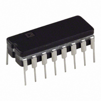
IC SGNL COND 4-20MA TX 16-CDIP

AD694AQ

Manufacturer Part Number
AD694AQ
Description
IC SGNL COND 4-20MA TX 16-CDIP
Manufacturer
Analog Devices Inc
Type
Current Transmitterr
Datasheet

Specifications of AD694AQ

Rohs Status
RoHS non-compliant
Input Type
Voltage
Output Type
Voltage
Current - Supply
23mA
Mounting Type
Through Hole
Package / Case
16-CDIP (0.300", 7.62mm)
No. Of Amplifiers
1
Input Offset Voltage
500µV
Bandwidth
300kHz
Amplifier Output
Single Ended
Cmrr
90dB
Supply Voltage Range
4.5V To 36V
Supply Current
1.5mA
Amplifier Case Style
DIP
Rohs Compliant
No
Interface
-

Available stocks

Company
Part Number
Manufacturer
Quantity
Price
Part Number:
AD694AQ
Manufacturer:
ADI
Quantity:
518
Company:
Part Number:
AD694AQ
Quantity:
1 000
a
PRODUCT DESCRIPTION
The AD694 is a monolithic current transmitter that accepts
high level signal inputs to drive a standard 4–20 mA current
loop for the control of valves, actuators, and other devices com-
monly used in process control. The input signal is buffered by
an input amplifier that can be used to scale the input signal or
buffer the output from a current mode DAC. Precalibrated in-
put spans of 0 V to 2 V and 0 V to 10 V are selected by simple
pin strapping; other spans may be programmed with external
resistors.
The output stage compliance extends to within 2 V of V
its special design allows the output voltage to extend below
common in dual supply operation. An alarm warns of an open
4–20 mA loop or noncompliance of the output stage.
Active laser trimming of the AD694’s thin film resistors results
in high levels of accuracy without the need for additional adjust-
ments and calibration. An external pass transistor may be used
with the AD694 to off-load power dissipation, extending the
temperature range of operation.
The AD694 is the ideal building block for systems requiring
noise immune 4–20 mA signal transmission to operate valves,
actuators, and other control devices, as well as for the transmis-
sion of process parameters such as pressure, temperature, or
flow. It is recommended as a replacement for discrete designs in
a variety of applications in industrial process control, factory
automation, and system monitoring.
The AD694 is available in hermetically sealed, 16-pin CERDIP
and plastic SOIC, specified over the –40°C to +85°C industrial
temperature range, and in a 16-pin plastic DIP, specified over
the 0°C to +70°C temperature range.
REV. B
Information furnished by Analog Devices is believed to be accurate and
reliable. However, no responsibility is assumed by Analog Devices for its
use, nor for any infringements of patents or other rights of third parties that
may result from its use. No license is granted by implication or otherwise
under any patent or patent rights of Analog Devices.
FEATURES
4–20 mA, 0–20 mA Output Ranges
Precalibrated Input Ranges:
Precision Voltage Reference
Single or Dual Supply Operation
Wide Power Supply Range: 4.5 V to 36 V
Wide Output Compliance
Input Buffer Amplifier
Open-Loop Alarm
Optional External Pass Transistor to Reduce
0.002% Typ Nonlinearity
0 V to 2 V, 0 V to 10 V
Programmable to 2.000 V or 10.000 V
Self-Heating Errors
S
and
PRODUCT HIGHLIGHTS
1. The AD694 is a complete voltage in to 4–20 mA out current
2. Pin programmable input ranges are precalibrated at 0 V to
3. The input amplifier may be configured to buffer and scale the
4. The output voltage compliance extends to within 2 V of the
5. The AD694 interfaces directly to 8-, 10-, and 12-bit single
6. The 4 mA zero current may be switched on and off with a
7. An open collector alarm warns of loop failure due to open
8. A monitored output is provided to drive an external pass
One Technology Way, P.O. Box 9106, Norwood, MA 02062-9106, U.S.A.
Tel: 781/329-4700
Fax: 781/326-8703
transmitter.
2 V and 0 V to 10 V.
input voltage, or to serve as an output amplifier for current
output DACs.
positive supply and below common. When operated with a
5 V supply, the output voltage compliance extends 30 V be-
low common.
supply CMOS and bipolar DACs.
TTL control pin, allowing 0–20 mA operation.
wires or noncompliance of the output stage.
transistor. The feature off-loads power dissipation to extend
the temperature range of operation and minimize self-heating
error.
FUNCTIONAL BLOCK DIAGRAM
4–20 mA Transmitter
© Analog Devices, Inc., 2002
AD694
www.analog.com

Related parts for AD694AQ

AD694AQ Summary of contents

Page 1

FEATURES 4–20 mA, 0–20 mA Output Ranges Precalibrated Input Ranges Precision Voltage Reference Programmable to 2.000 V or 10.000 V Single or Dual Supply Operation Wide Power Supply Range: ...

Page 2

... Alarm Pin Current (Pin 10) POWER REQUIREMENTS Specified Performance Operating Range REF FS REF Quiescent Current Off TEMPERATURE RANGE 5 Specified Performance AD694AQ/BQ/AR/BR –40 AD694JN Operating AD694AQ/BQ/AR/BR –55 AD694JN (@ + 250 , and V = +24 V, unless otherwise noted AD694JN/AQ/AR Min Typ Max Min –0.2 V –2 –2.5 V –0.2 ...

Page 3

... All pins are rated for a minimum of 4000 V protection, except for Pins 2, 3 and 9 which are rated to survive a minimum of 1500 V. ESD testing conforms to Human Body Model. Always practice ESD prevention. (13). S Model AD694JN AD694AQ AD694AR AD694BQ AD694BR *N = Plastic DIP CERDIP SOIC –3– AD694 AD694BQ/BR ...

Page 4

AD694 Typical Minimum Supply Voltage vs. Temperature for 2 V and 10 V Full Scale Maximum R vs. Supply Voltage L Voltage Reference Power Supply Rejection I : Voltage Compliance vs. Temperature OUT FUNCTIONAL DESCRIPTION The operation of the AD694 ...

Page 5

NPN pass transistor can be added to transfer most of the power dissipation off-chip, to extend the temperature range of operation. The output stage is current-limited at approximately protect the output from an overdrive at its ...

Page 6

AD694 An NPN boost transistor can be added in the 2 V mode to in- crease the current drive capability of the 2 V reference. The 10 V force pin is connected to the base of the NPN, and the ...

Page 7

Figure 4. Using Optional Pass Transistor to Minimize Self-Heating Errors; Dual Supply Operation Shown POWER DISSIPATION CONSIDERATIONS The AD694 is rated for operation over its specified temperature without the use of an external pass transistor. However possible to ...

Page 8

AD694 Figure 6 will give an approximately linear adjustment of the 4 mA offset within fixed limits. To find the proper resistor val- ues, first select X, the desired range of adjustment as a fraction of 4 mA. Substitute this ...

Page 9

Figure 8. Span Adjustment Full Scale PROGRAMMING OTHER SPANS There are two methods for programming input spans less than 10 V. The first decreases the input span by programming a non- inverting gain into the buffer amplifier. For ...

Page 10

AD694 Figure 11. Buffer Amplifier V APPLICATIONS CURRENT OUTPUT DAC INTERFACE The AD694 can be easily interfaced to current output DACs such as the AD566A to construct a digital to 4–20 mA interface as shown in Figure 13. The AD694 ...

Page 11

Figure 13. Digital to 4–20 mA Interface Using a Current Steering DAC Figure 14. Single-Supply Digital Input to 4–20 mA Output code dependent, and the response time of the circuit will be de- termined by the reaction of the voltage ...

Page 12

AD694 The circuit shown, will convert a positive differential signal 4–20 mA current. The circuit has common-mode range The low end of the common-mode range is limited by the ...

Page 13

Ceramic DIP-Glass Hermetic Seal Package [CERDIP] 5.08 (0.2000) MAX 5.08 (0.2000) 3.18 (0.1252) 0.58 (0.0228) 0.36 (0.0142) 5.33 (0.2098) 4.06 (0.1598) 2.93 (0.1154) 0.30 (0.0118) 0.10 (0.0039) COPLANARITY REV. B OUTLINE DIMENSIONS (Q-16) Dimensions shown in millimeters and (inches) ...

Page 14

AD694 Revision History Location 8/02—Data Sheet changed from REV REV. B. Updated Outline Dimensions . . . . . . . . . . . . . . . . . . . . . . . . ...

Page 15

REV. B –15– ...

Page 16

–16– ...

Related keywords