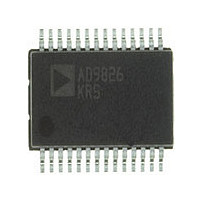
AD9826KRS Analog Devices Inc, AD9826KRS Datasheet - Page 15

AD9826KRS
Manufacturer Part Number
AD9826KRS
Description
IC IMAGE SGNL PROC 16BIT 28-SSOP
Manufacturer
Analog Devices Inc
Type
Image Sensorr
Datasheet
1.AD9826KRSZRL.pdf
(20 pages)
Specifications of AD9826KRS
Rohs Status
RoHS non-compliant
Input Type
Logic
Output Type
Logic
Interface
3-Wire Serial
Current - Supply
75mA
Mounting Type
Surface Mount
Package / Case
28-SSOP
Analog Front End Type
CCD
Analog Front End Category
Video
Interface Type
Serial (3-Wire)
Sample Rate
30MSPS
Input Voltage Range
2V
Operating Supply Voltage (min)
3/4.75V
Operating Supply Voltage (typ)
5V
Operating Supply Voltage (max)
5.25V
Resolution
16b
Supply Current
5/75mA
Number Of Adc's
1
Power Supply Type
Analog/Digital
Operating Temp Range
-40C to 85C
Operating Temperature Classification
Industrial
Mounting
Surface Mount
Pin Count
28
Package Type
SSOP
Number Of Channels
3
Lead Free Status / RoHS Status
Not Compliant
Available stocks
Company
Part Number
Manufacturer
Quantity
Price
Part Number:
AD9826KRS
Manufacturer:
ADI/亚德诺
Quantity:
20 000
Company:
Part Number:
AD9826KRSRL
Manufacturer:
MAXIM
Quantity:
94 126
Part Number:
AD9826KRSRL
Manufacturer:
ADI/亚德诺
Quantity:
20 000
Company:
Part Number:
AD9826KRSZ
Manufacturer:
AD
Quantity:
5 510
Part Number:
AD9826KRSZ
Manufacturer:
ADI/亚德诺
Quantity:
20 000
Part Number:
AD9826KRSZ-REEL
Manufacturer:
ADI/亚德诺
Quantity:
20 000
Part Number:
AD9826KRSZRL
Manufacturer:
ADI/亚德诺
Quantity:
20 000
MUX Configuration Register
The MUX Configuration Register controls the sampling chan-
nel order and the 2-Channel Mode configuration in the AD9826.
Bits D8 and D3–D0 should always be set low. Bit D7 is used
when operating in 3-Channel or 2-Channel Mode. Setting Bit
D7 high will sequence the MUX to sample the Red channel
first, then the Green channel, and then the Blue channel. When
in 3-channel mode, the CDSCLK2 pulse always resets the MUX
to sample the Red channel first (see Figure 11). When Bit D7 is
set low, the channel order is reversed to Blue first, Green sec-
ond, and Red third. The CDSCLK2 pulse will always reset the
MUX to sample the Blue channel first. Bits D6, D5, and D4 are
used when operating in 1 or 2-Channel Mode. Bit D6 is set high
to sample the Red channel. Bit D5 is set high to sample the
Green channel. Bit D4 is set high to sample the Blue channel.
The MUX will remain stationary during 1-channel mode. Two-
Channel Mode is selected by setting two of the channel select
Bits (D4–D6) high. The MUX samples the channels in the
order selected by Bit D7.
D
Set
to
0
D8
Set to 0
0
0
0
0
D8
MSB
0
0
0
1
1
1
Power-on default value.
Power-on default value.
Power-on default value.
8
D7
MUX Order
1 = R-G-B
0 = B-G-R
D7
Set to 0
0
0
0
0
D7
0
0
1
0
0
1
D6
Set to 0
0
0
0
0
D6
Channel Select
1 = RED
0 = Off
D6
0
0
1
0
0
1
D5
MSB
0
0
1
1
D5
0
0
1
0
0
1
Table III. MUX Configuration Register Settings
D4
0
0
1
1
D5
Channel Select
1 = GREEN
0 = Off
Table IV. PGA Gain Register Settings
•
•
•
D4
0
0
1
0
0
1
Table V. Offset Register Settings
D3
0
0
1
1
•
•
•
•
•
•
D3
0
0
1
0
0
1
D4
Channel Select
1 = BLUE
0 = Off
D2
0
0
1
1
PGA Gain Registers
There are three PGA registers for individually programming the
gain in the Red, Green, and Blue channels. Bits D8, D7, and
D6 in each register must be set low, and Bits D5 through D0
control the gain range from 1 to 6 in 64 increments. See
Figure 17 for a graph of the PGA gain versus PGA register
code. The coding for the PGA registers is straight binary, with
an all “zeros” word corresponding to the minimum gain setting
(1 ) and an all “ones” word corresponding to the maximum
gain setting (6 ).
Offset Registers
There are three Offset Registers for individually programming
the offset in the Red, Green, and Blue channels. Bits D8 through
D0 control the offset range from –300 mV to +300 mV in 512
increments. The coding for the Offset Registers is Sign Mag-
nitude, with D8 as the sign bit. Table V shows the offset range
as a function of the Bits D8 through D0.
D2
0
1
0
1
0
0
D1
0
0
1
1
D0
LSB
0
1
1
1
D1
0
0
1
0
0
1
D3
Set
to
0
D0
LSB
0
1
1
0
1
1
to
0
Set
D2
Gain (V/V)
1.0
1.013
5.56
6.0
•
•
•
D1
to
0
Set
Offset (mV)
0
+1.2
+300
0
–1.2
–300
AD9826
•
•
•
•
•
•
Gain (dB)
0.0
0.12
14.9
15.56
•
•
•
D0
Set
to
0


