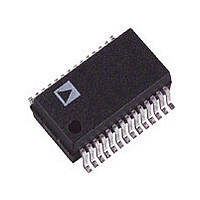
AD9826KRSRL Analog Devices Inc, AD9826KRSRL Datasheet - Page 17

AD9826KRSRL
Manufacturer Part Number
AD9826KRSRL
Description
IC IMAGE SGNL PROC 16BIT 28-SSOP
Manufacturer
Analog Devices Inc
Type
Image Sensorr
Datasheet
1.AD9826KRSZRL.pdf
(20 pages)
Specifications of AD9826KRSRL
Rohs Status
RoHS non-compliant
Input Type
Logic
Output Type
Logic
Interface
3-Wire Serial
Current - Supply
75mA
Mounting Type
Surface Mount
Package / Case
28-SSOP
Analog Front End Type
CCD
Analog Front End Category
Video
Interface Type
Serial (3-Wire)
Sample Rate
30MSPS
Input Voltage Range
2V
Operating Supply Voltage (min)
3/4.75V
Operating Supply Voltage (typ)
5V
Operating Supply Voltage (max)
5.25V
Resolution
16b
Supply Current
5/75mA
Number Of Adc's
1
Power Supply Type
Analog/Digital
Operating Temp Range
-40C to 85C
Operating Temperature Classification
Industrial
Mounting
Surface Mount
Pin Count
28
Package Type
SSOP
Number Of Channels
3
Lead Free Status / RoHS Status
Not Compliant
Available stocks
Company
Part Number
Manufacturer
Quantity
Price
Company:
Part Number:
AD9826KRSRL
Manufacturer:
MAXIM
Quantity:
94 126
Part Number:
AD9826KRSRL
Manufacturer:
ADI/亚德诺
Quantity:
20 000
Analog Inputs—
Figure 14 shows the analog input configuration for the SHA
mode of operation. Figure 15 shows the internal timing for the
sampling switches. The input signal is sampled when CDSCLK2
transitions from high to low, opening S1. The voltage on the
OFFSET pin is also sampled on the falling edge of CDSCLK2,
when S2 opens. S3 is then closed, generating a differential out-
put voltage representing the difference between the sampled
input voltage and the OFFSET voltage. The input clamp is
disabled during SHA mode operation.
(INTERNAL)
OPTIONAL DC
CDSCLK2
OFFSET (OR
CONNECT
TO GND)
SIGNAL
Q3
INPUT
S1, S2 OPEN
OFFSET
VINB
S3 OPEN
SHA Mode Operation
VING
VINR
AD9826
S1, S2 CLOSED
S3 CLOSED
S2
S1
S3
S1, S2 CLOSED
4pF
S3 CLOSED
4pF
CML
CML
Figure 16 shows how the OFFSET pin may be used in a CIS
application for coarse offset adjustment. Many CIS signals have
dc offsets ranging from several hundred millivolts to more than
1 V. By connecting the appropriate dc voltage to the OFFSET
pin, the CIS signal will be restored to “zero.” After the large dc
offset is removed, the signal can be scaled using the PGA to
maximize the ADC’s dynamic range.
DC OFFSET
CIS MODULE
VRED FROM
R2
R1
AVDD
GREEN
BLUE
RED
OFFSET
0.1 F
VING
VINR
VINB
AD9826
SHA
SHA
SHA
AD9826
RED-
OFFSET
GREEN-
OFFSET
BLUE-
OFFSET


