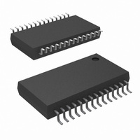
DS92LV1224TMSA/NOPB National Semiconductor, DS92LV1224TMSA/NOPB Datasheet

DS92LV1224TMSA/NOPB
Specifications of DS92LV1224TMSA/NOPB
*DS92LV1224TMSA/NOPB
DS92LV1224TMSA
Related parts for DS92LV1224TMSA/NOPB
DS92LV1224TMSA/NOPB Summary of contents
Page 1
... The DS92LV1023 was designed with the flow-through pinout and is available in a space saving 28–lead SSOP package. Block Diagrams TRI-STATE ® registered trademark of National Semiconductor Corporation. © 2005 National Semiconductor Corporation Features n 40–66 MHz Single 10:1 Serializer with 400–660 Mb/s throughput ...
Page 2
Block Diagrams (Continued) Functional Description The DS92LV1023 is a 10-bit Serializer device which together with a compatible deserializer (i.e. DS92LV1224) forms a chipset designed to transmit data over FR-4 printed circuit board backplanes and balanced copper cables at clock speeds ...
Page 3
Data Transfer (Continued) clock and uses it to recover the serialized data. ROUT data is valid when LOCK is low. Otherwise ROUT0–ROUT9 is invalid. The ROUT0-ROUT9 pins use the RCLK pin as the reference to data. The polarity of the ...
Page 4
Ordering Information NSID DS92LV1023TMSA DIN0 Held Low-DIN1 Held High Creates an RMT Pattern DIN4 Held Low-DIN5 Held High Creates an RMT Pattern FIGURE 1. RMT Patterns Seen on the Bus LVDS Serial Output www.national.com Function Serializer 10093324 DIN8 Held Low-DIN9 ...
Page 5
... Absolute Maximum Ratings If Military/Aerospace specified devices are required, please contact the National Semiconductor Sales Office/ Distributors for availability and specifications. Supply Voltage ( LVCMOS/LVTTL Input Voltage −0. LVCMOS/LVTTL Output Voltage −0. Bus LVDS Driver Output Voltage Bus LVDS Output Short Circuit Duration ...
Page 6
Serializer Timing Requirements for TCLK Over recommended operating supply and temperature ranges unless otherwise specified. Symbol Parameter t Transmit Clock Period TCP t Transmit Clock High Time TCIH t Transmit Clock Low Time TCIL t TCLK Input Transition CLKT Time ...
Page 7
AC Timing Diagrams and Test Circuits FIGURE 2. “Worst Case” Serializer ICC Test Pattern FIGURE 3. Serializer Bus LVDS Output Load and Transition Times FIGURE 4. Serializer Input Clock Transition Time Timing shown for TCLK_R/F = LOW FIGURE 5. Serializer ...
Page 8
AC Timing Diagrams and Test Circuits FIGURE 6. Serializer TRI-STATE Test Circuit and Timing FIGURE 7. Serializer PLL Lock Time, and PWRDN TRI-STATE Delays www.national.com (Continued) 10093309 8 10093310 ...
Page 9
AC Timing Diagrams and Test Circuits (Continued) FIGURE 8. SYNC Timing Delays FIGURE 9. Serializer Delay 9 10093323 10093311 www.national.com ...
Page 10
AC Timing Diagrams and Test Circuits + − (DO )–( Differential output signal is shown as (DO+)–(DO−), device in Data Transfer mode. Application Information USING THE SERIALIZER AND DESERIALIZER CHIPSET The Serializer and Deserializer chipset is ...
Page 11
FIGURE 11. Random Lock Hot Insertion 11 10093317 www.national.com ...
Page 12
Pin Diagrams Serializer Pin Description Pin Name I/O DIN I TCLK_R/F I DO+ O DO− O DEN I PWRDN I TCLK I SYNC I DVCC I DGND I AVCC I AGND I www.national.com DS92LV1023TMSA - Serializer 10093318 No. 3–12 Data ...
Page 13
... BANNED SUBSTANCE COMPLIANCE National Semiconductor manufactures products and uses packing materials that meet the provisions of the Customer Products Stewardship Specification (CSP-9-111C2) and the Banned Substances and Materials of Interest Specification (CSP-9-111S2) and contain no ‘‘Banned Substances’’ as defined in CSP-9-111S2. ...


