DS90CR486VS/NOPB National Semiconductor, DS90CR486VS/NOPB Datasheet
DS90CR486VS/NOPB
Specifications of DS90CR486VS/NOPB
*DS90CR486VS/NOPB
DS90CR486VS
Available stocks


Related parts for DS90CR486VS/NOPB

DS90CR486VS/NOPB Summary of contents
Page 1
... ISI (Inter-Symbol Interference). With pre-emphasis and DC balancing, a low distortion eye-pattern Generalized Block Diagram © 2006 National Semiconductor Corporation is provided at the receiver end of the cable. A cable deskew capability has been added to deskew long cables of pair-to- pair skew. These three enhancements allow long cables to be driven ...
Page 2
... Absolute Maximum Ratings If Military/Aerospace specified devices are required, please contact the National Semiconductor Sales Office/ Distributors for availability and specifications. Supply Voltage ( LVCMOS/LVTTL Output Voltage LVDS Receiver Input Voltage Junction Temperature Storage Temperature Lead Temperature (Soldering, 4 sec.) Maximum Package Power Dissipation Capacity @ 25° ...
Page 3
Receiver Switching Characteristics Over recommended operating supply and temperature ranges unless otherwise specified. Symbol Parameter CLHT LVCMOS/LVTTL Low-to-High Transition Time, (Figure 2), Rx data out, (Note 5) LVCMOS/LVTTL Low-to-High Transition Time, (Figure 2), Rx clock out, (Note 5) CHLT LVCMOS/LVTTL ...
Page 4
AC Timing Diagrams Note 7: The worst case test pattern produces a maximum toggling of digital circuits, LVDS I/O and LVCMOS/LVTTL I/O. FIGURE 2. DS90CR486 LVCMOS/LVTTL Output Load and Transition Times FIGURE 3. DS90CR486 Setup/Hold and High/Low Times www.national.com FIGURE ...
Page 5
FIGURE 4. DS90CR486 Propagation Delay - Latency FIGURE 5. DS90CR486 Phase Lock Loop Set Time (V FIGURE 6. DS90CR486 Power Down Delay 5 20025228 20025220 > 3.0V) CC 20025222 www.national.com ...
Page 6
C—Setup and Hold Time (Internal data sampling window) defined by Rspos (receiver input strobe position) min and max Tppos—Transmitter output pulse position (min and max) RSKMD = ISI (Inter-symbol interference) + TPPOS(variance) + LVDS Source Clock Jitter (cycle to cycle) ...
Page 7
LVDS Interface FIGURE 8. 48 LVCMOS/LVTTL Outputs Mapped to 8 LVDS Inputs (DC Balance Mode- Disable, BAL = Low) (E1 - Falling Edge Rising Edge) 7 20025204 www.national.com ...
Page 8
FIGURE 9. 48 LVCMOS/LVTTL Outputs Mapped to 8 LVDS Inputs(DC Balance Mode - Enable, BAL = High) www.national.com (E1 - Falling Edge Rising Edge) 8 20025257 ...
Page 9
DS90CR486 Outputs Mapped to DS90CR485 Outputs/DS90CR483 Inputs DS90CR486 Receiver Output RxOUT0 RxOUT1 RxOUT2 RxOUT3 RxOUT4 RxOUT5 RxOUT6 RxOUT7 RxOUT8 RxOUT9 RxOUT10 RxOUT11 RxOUT12 RxOUT13 RxOUT14 RxOUT15 RxOUT16 RxOUT17 RxOUT18 RxOUT19 RxOUT20 RxOUT21 RxOUT22 RxOUT23 RxOUT24 RxOUT25 RxOUT26 RxOUT27 RxOUT28 RxOUT29 ...
Page 10
DS90CR486 Receiver Output RxOUT47 * E1 = Falling Edge and E2 = Rising Edge of RxCLK P/M Input Clock Edge www.national.com DS90CR485 Transmitter Input * E1-D23 10 DS90CR483 Transmitter Input TxIN47 ...
Page 11
DS90CR486 Pin Descriptions — Channel Link Receiver Pin Name I/O RxINP I RxINM I RxOUT O RxCLKP I RxCLKM I RxCLKOUT O PLLSEL DESKEW I BAL I CON1 GND I PLLV I CC ...
Page 12
Applications Information DC BALANCE In addition to data information an additional bit is transmitted on every LVDS data signal line during each cycle as shown in Figure 9. This bit is the DC balance bit (DCB). The purpose of the ...
Page 13
The transmitter-DS90CR485 “DS_OPT” pin may be set high backplane application with short PCB dis- tance traces, pre-emphasis from the transmitter is typically not required. The “PRE” pin should be left open (do not tie to ground). ...
Page 14
CONFIGURATION 1 DS90CR481/483 and DS90CR484 with DC Balance ON (BAL=High, 33MHz to 80MHz) − The DS_OPT pin at the input of the transmitter DS90CR481/483 must be applied low for a minimum of four clock cycles in order for the receiver ...
Page 15
Pin Diagram Receiver - DS90CR486 (Top View) 15 20025207 www.national.com ...
Page 16
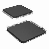
Physical Dimensions www.national.com inches (millimeters) unless otherwise noted Dimensions show in millimeters Order Number DS90CR486VS NS Package Number VS100A 16 ...
Page 17
Notes 17 www.national.com ...
Page 18
... National Semiconductor and the National Semiconductor logo are registered trademarks of National Semiconductor Corporation. All other brand or product names may be trademarks or registered trademarks of their respective holders. ...