CLC020BCQ/NOPB National Semiconductor, CLC020BCQ/NOPB Datasheet - Page 3
CLC020BCQ/NOPB
Manufacturer Part Number
CLC020BCQ/NOPB
Description
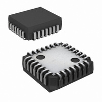
IC SERIALIZER VIDEO DGTL 28-PLCC
Manufacturer
National Semiconductor
Datasheet
1.CLC020BCQNOPB.pdf
(15 pages)
Specifications of CLC020BCQ/NOPB
Function
Serializer
Data Rate
400Mbps
Input Type
CMOS
Output Type
CMOS, TTL
Number Of Inputs
10
Number Of Outputs
1
Voltage - Supply
4.5 V ~ 5.5 V
Operating Temperature
0°C ~ 70°C
Mounting Type
Surface Mount
Package / Case
28-PLCC
For Use With
SD020EVK - BOARD EVALUATION CLC020
Lead Free Status / RoHS Status
Lead free / RoHS Compliant
Other names
*CLC020BCQ
*CLC020BCQ/NOPB
CLC020BCQ
*CLC020BCQ/NOPB
CLC020BCQ
Available stocks
Company
Part Number
Manufacturer
Quantity
Price
Company:

Part Number:
CLC020BCQ/NOPB
Manufacturer:
National Semiconductor
Quantity:
135
Company:
Part Number:
CLC020BCQ/NOPB
Manufacturer:
LT
Quantity:
4 067
Company:
Part Number:
CLC020BCQ/NOPB
Manufacturer:
Texas Instruments
Quantity:
10 000


Symbol
V
V
I
I
V
V
V
I
Symbol
BR
F
t
t
t
t
t
t
IH
IL
DD
r
j
jit
r
LOCK
SU
, t
, t
IH
IL
OH
OL
SDO
P CLK
Absolute Maximum Ratings
If Military/Aerospace specified devices are required,
please contact the National Semiconductor Sales Office/
Distributors for availability and specifications.
DC Electrical Characteristics
Over Supply Voltage and Operating Temperature ranges, unless otherwise specified (Notes 2, 3).
AC Electrical Characteristics
Over Supply Voltage and Operating Temperature ranges, unless otherwise specified (Note 3).
Supply Voltage (V
CMOS/TTL Input Voltage (V
CMOS/TTL Output Voltage (V
CMOS/TTL Input Current (single input)
Input Current, Other Inputs
CMOS/TTL Output Source/Sink Current
SDO Output Source Current
Package Thermal Resistance
Storage Temp. Range
SDO
f
f
V
V
θ
θ
JA
JC
I
I
= V
= V
28-lead PLCC
28-lead PLCC
SS
DD
Parameter
Input Voltage High Level
Input Voltage Low Level
Input Current High Level
Input Current Low Level
CMOS Output Voltage
High Level
CMOS Output Voltage
Low Level
Serial Driver Output
Voltage
Power Supply Current,
Total
Parameter
Serial data rate
Reference Clock
Input Frequency
Reference Clock Duty
Cycle
Rise time, Fall time
Serial output jitter
Serial output jitter
Rise time, Fall time
Output overshoot
Lock time
Setup time
−0.5V
+0.5V
DD
−V
SS
)
I
)
O
)
Conditions
R
10%–90%
270 Mbps,Figure 2, (Note 6)
(Notes 4, 5)
20%–80%, (Notes 4, 5)
270 Mbps, (Notes 5, 7)
Figure 3
−0.5V to (V
−0.5V to (V
L
Conditions
V
V
I
I
R
R
Figure 2
R
R
P
NTSC Colour Bar Pattern
OH
OL
= 75Ω, AC coupled, (Note 5)
IH
IL
CLK
L
REF
L
REF
= 75Ω 1%,
= 75Ω 1%,
= V
= +10 mA
−65˚C to +150˚C
= V
= −10 mA
= 27 MHz, Figure 2,
= 1.69 kΩ 1%,
= 1.69 kΩ 1%,
SS
DD
(Note 1)
DD
DD
±
85˚C/W
35˚C/W
+ 0.5V)
+ 0.5V)
±
−5 mA
+5 mA
10 mA
20 mA
1 mA
6.0V
3
Recommended Operating
Conditions
Junction Temperature
Lead Temperature (Soldering 4 Sec)
ESD Rating (HBM)
ESD Rating (MM)
Transistor Count
Supply Voltage (V
CMOS/TTL Input Voltage
P
P
D
Maximum DC Bias on SDO pins
Operating Free Air Temperature (T
Reference
D0 through D9,
P
and Sync.
Detect Enable
Lock Detect,
Test Out
SDO, SDO
CLK
CLK
CLK
N
and P
, TPG_EN
Reference
SDO, SDO
P
P
D
SDO, SDO
D
Frequency Range
Duty Cycle
CLK
CLK
N
N
, P
to P
CLK
CLK
CLK
Rise/Fall Time
DD
−V
Min
V
700
2.0
2.4
0.0
SS
SS
)
Min
100
500
1.0
10
45
3
Typ
+40
800
4.7
0.3
47
-1
Typ
220
100
800
1.5
50
75
A
1
2
)
V
SS
Max
V
V
+60
900
0.8
-20
60
+ 0.5V
DD
DD
1500
Max
400
200
3.0
40
55
0˚C to +70˚C
10 to 40MHz
1.0 to 3.0 ns
5.0V
3.0V
V
www.national.com
45 to 55%
SS
>
>
+150˚C
+260˚C
33,400
to V
2.5 kV
200 V
±
±
mV
Units
Mbps
Units
ps
ps
MHz
10%
10%
mA
µA
µA
ns
ps
µs
ns
%
%
V
V
V
V
P-P
P-P
DD
P-P
Related parts for CLC020BCQ/NOPB
Image
Part Number
Description
Manufacturer
Datasheet
Request
R

Part Number:
Description:
Buffer / Driver / Receiver Logic IC
Manufacturer:
National Semiconductor

Part Number:
Description:
BOARD EVALUATION CLC020
Manufacturer:
National Semiconductor
Datasheet:
Part Number:
Description:
National Semiconductor [8-Bit D/A Converter]
Manufacturer:
National Semiconductor
Datasheet:
Part Number:
Description:
National Semiconductor [Media Coprocessor]
Manufacturer:
National Semiconductor
Datasheet:
Part Number:
Description:
Digitally Controlled Tone and Volume Circuit with Stereo Audio Power Amplifier, Microphone Preamp Stage and National 3D Sound
Manufacturer:
National Semiconductor
Datasheet:
Part Number:
Description:
Digitally Controlled Tone and Volume Circuit with Stereo Audio Power Amplifier, Microphone Preamp Stage and National 3D Sound
Manufacturer:
National Semiconductor
Datasheet:
Part Number:
Description:
AC97 Rev 2 Codec with Sample Rate Conversion and National 3D Sound
Manufacturer:
National Semiconductor
Part Number:
Description:
Manufacturer:
National Semiconductor
Datasheet:
Part Number:
Description:
Manufacturer:
National Semiconductor
Datasheet:
Part Number:
Description:
General Purpose, Low Voltage, Low Power, Rail-to-Rail Output Operational Amplifiers
Manufacturer:
National Semiconductor
Datasheet:
Part Number:
Description:
8-bit 20 MSPS flash A/D converter.
Manufacturer:
National Semiconductor
Datasheet:
Part Number:
Description:
Low Noise Quad Operational Amplifier
Manufacturer:
National Semiconductor
Datasheet:
Part Number:
Description:
Quad Differential Line Receivers
Manufacturer:
National Semiconductor
Datasheet:
Part Number:
Description:
Quad High Speed Trapezoidal? Bus Transceiver
Manufacturer:
National Semiconductor
Datasheet: