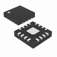
MAX9226ETE+ Maxim Integrated Products, MAX9226ETE+ Datasheet

MAX9226ETE+
Specifications of MAX9226ETE+
Related parts for MAX9226ETE+
MAX9226ETE+ Summary of contents
Page 1
... LATCH PIXEL CLOCK IN CONTROL MAX9225 ________________________________________________________________ Maxim Integrated Products For pricing, delivery, and ordering information, please contact Maxim Direct at 1-888-629-4642, or visit Maxim’s website at www.maxim-ic.com. ♦ Ideal for Serializing Cell Phone Camera Parallel Interface ♦ MAX9225 Serializes 8-Bit YUV, HSYNC, and VSYNC ♦ ...
Page 2
Low-Power, 10MHz-to-20MHz Serializer and Deserializer Chipset ABSOLUTE MAXIMUM RATINGS V to GND ...........................................................-0.5V to +4. GND.........................................................-0.5V to +4.0V DDO Serial Interface (SDO+, SDO-, SDI+, SDI-) to GND .....................................................-0.5V to +4.0V Single-Ended Inputs (DIN_, PCLKIN, PWRDN) to ...
Page 3
Low-Power, 10MHz-to-20MHz Serializer and Deserializer Chipset DC ELECTRICAL CHARACTERISTICS (MAX9226 +2.375V to +3.465V +1.71V to +3.465V DDO V = +2.5V +25°C.) (Notes 1, 2) DDO A PARAMETER SYMBOL SINGLE-ENDED OUTPUTS (PCLKOUT, ...
Page 4
Low-Power, 10MHz-to-20MHz Serializer and Deserializer Chipset AC ELECTRICAL CHARACTERISTICS (MAX9225 +2.375V to +3.465V -40°C to +85°C, unless otherwise noted. Typical values are PARAMETER SYMBOL PCLKIN INPUT REQUIREMENTS (Figure 3) Input Rise ...
Page 5
Low-Power, 10MHz-to-20MHz Serializer and Deserializer Chipset ODD DIN_ EVEN DIN_ PCLKIN Figure 1. Serializer Worst-Case Switching Pattern V IH PCLKIN DIN_ PWRDN V IS THE MAXIMUM LOW-LEVEL INPUT (SEE THE DC ELECTRICAL CHARACTERISTICS TABLE) V ...
Page 6
Low-Power, 10MHz-to-20MHz Serializer and Deserializer Chipset ( +2.8V, logic input levels = 0 to +2.8V, logic output load C DD DDO MAX9225 SUPPLY CURRENT vs. SUPPLY VOLTAGE 10 DIN[9:0] = ALL LOW PCLKIN = 20MHz 8 ...
Page 7
Low-Power, 10MHz-to-20MHz Serializer and Deserializer Chipset ( +2.8V, logic input levels = 0 to +2.8V, logic output load C DD DDO MAX9226 SUPPLY CURRENT vs. SUPPLY VOLTAGE 11 DIN[9:0] = WORST-CASE SWITCHING PATTERN 10 PCLKOUT = ...
Page 8
Low-Power, 10MHz-to-20MHz Serializer and Deserializer Chipset PIN NAME 1–7, DIN6–DIN0, Single-Ended Parallel Data Inputs. The 10 data bits are loaded into the input latch on the rising 14, 15, 16 DIN9, DIN8, DIN7 edge of PCLKIN. 1.71V to 3.465V ...
Page 9
Low-Power, 10MHz-to-20MHz Serializer and Deserializer Chipset Functional Diagram (MAX9225) INPUT DIN[9:0] LATCH TIMING PCLKIN AND CONTROL DLL MAX9225 Detailed Description The MAX9225 serializer operates at a 10MHz-to-20MHz parallel clock frequency, serializing 10 bits of parallel input data DIN[9:0] in ...
Page 10
Low-Power, 10MHz-to-20MHz Serializer and Deserializer Chipset PARALLEL DATA INPUT PCLK IN DIN[9:0] DIN EXAMPLE INPUT LCDS SERIAL-DATA OUTPUT FOR EXAMPLE INPUT (SD0+/SDO NOTE: OH1 AND OH2 ARE OPPOSITE POLARITY. Figure 5. Multilevel LCDS Output Representation Applications ...
Page 11
Low-Power, 10MHz-to-20MHz Serializer and Deserializer Chipset POWER-UP AND LINK IN POWER- SYNCHRONIZATION DOWN PWRDN 1 2 PCLKIN DON'T CARE DIN_ DOUT_ PCLKOUT Figure 6. MAX9225/MAX9226 Power-Up/Power-Down Sequence Flex Cable, PCB Interconnect, Interconnect for LCDS typically has a differential imped- ...
Page 12
Low-Power, 10MHz-to-20MHz Serializer and Deserializer Chipset TOP VIEW DIN9 MAX9225 DIN8 15 DIN7 TQFN-EP 12 ______________________________________________________________________________________ PCLKIN DOUT7 DIN0 14 DOUT8 DIN1 6 DOUT9 ...
Page 13
Low-Power, 10MHz-to-20MHz Serializer and Deserializer Chipset (The package drawing(s) in this data sheet may not reflect the most current specifications. For the latest package outline information www.maxim-ic.com/packages.) E MARKING E/2 AAAA D 0.10 C ...
Page 14
Low-Power, 10MHz-to-20MHz Serializer and Deserializer Chipset (The package drawing(s) in this data sheet may not reflect the most current specifications. For the latest package outline information www.maxim-ic.com/packages.) PKG 8L 3x3 12L 3x3 REF. MIN. NOM. MAX. MIN. ...
Page 15
... Maxim cannot assume responsibility for use of any circuitry other than circuitry entirely embodied in a Maxim product. No circuit patent licenses are implied. Maxim reserves the right to change the circuitry and specifications without notice at any time. Maxim Integrated Products, 120 San Gabriel Drive, Sunnyvale, CA 94086 408-737-7600 ____________________ 15 © 2007 Maxim Integrated Products ...


