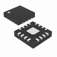
MAX9226ETE+ Maxim Integrated Products, MAX9226ETE+ Datasheet - Page 8

MAX9226ETE+
Manufacturer Part Number
MAX9226ETE+
Description
IC DESERIALIZER LP 16-TQFN
Manufacturer
Maxim Integrated Products
Datasheet
1.MAX9226ETE.pdf
(15 pages)
Specifications of MAX9226ETE+
Function
Serializer/Deserializer
Data Rate
200Mbps
Input Type
Parallel
Output Type
Parallel
Number Of Inputs
1
Number Of Outputs
10
Voltage - Supply
2.375 V ~ 3.465 V
Operating Temperature
-40°C ~ 85°C
Mounting Type
Surface Mount
Package / Case
16-TQFN Exposed Pad
Lead Free Status / RoHS Status
Lead free / RoHS Compliant
10-Bit, Low-Power, 10MHz-to-20MHz
Serializer and Deserializer Chipset
8
14, 15, 16
_______________________________________________________________________________________
6–15
1–7,
PIN
PIN
10
11
12
13
16
—
—
8
9
1
2
3
4
5
DIN9, DIN8, DIN7
DOUT0–DOUT9
DIN6–DIN0,
PCLKOUT
PCLKIN
PWRDN
NAME
NAME
SDO+
V
SDO-
GND
GND
SDI+
SDI-
V
V
DDO
EP
EP
DD
DD
Single-Ended Parallel Data Inputs. The 10 data bits are loaded into the input latch on the rising
edge of PCLKIN. 1.71V to 3.465V tolerant. Internally pulled down to GND.
Parallel Clock Input. The rising edge of PCLKIN (typically the pixel clock) latches the parallel
data input. Internally pulled down to GND.
Power-Down Input. Pull PWRDN low to place the MAX9225/MAX9226 in power-down mode.
Drive PWRDN high for normal operation. Internally pulled down to GND.
Inverting LCDS Serial-Data Output
Noninverting LCDS Serial-Data Output
Ground
Core Supply Voltage. Bypass to GND with 0.1µF and 0.01µF capacitors in parallel as close to
the device as possible with the smallest value capacitor closest to the supply pin.
Exposed Paddle. Connect EP to ground.
Ground
Noninverting LCDS Serial-Data Input
Inverting LCDS Serial-Data Input
Core Supply Voltage. Bypass to GND with 0.1µF and 0.01µF capacitors in parallel as close to
the device as possible, with the smallest value capacitor closest to the supply pin.
Parallel Clock Output. Parallel output data are valid on the rising edge of PCLKOUT (typically
the pixel clock).
Single-Ended Parallel Data Output. DOUT[9:0] are valid on the rising edge of PCLKOUT.
Output Supply Voltage. Bypass to GND with 0.1µF and 0.01µF capacitors in parallel as close to
the device as possible with the smallest value capacitor closest to the supply pin.
Exposed Paddle. Connect EP to ground.
FUNCTION
FUNCTION
Pin Description (MAX9225)
Pin Description (MAX9226)


