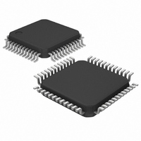
MAX9248ECM/V+ Maxim Integrated Products, MAX9248ECM/V+ Datasheet - Page 17

MAX9248ECM/V+
Manufacturer Part Number
MAX9248ECM/V+
Description
IC DESERIALIZER LVDS 48-LQFP
Manufacturer
Maxim Integrated Products
Datasheet
1.MAX9250ECMT.pdf
(20 pages)
Specifications of MAX9248ECM/V+
Function
Deserializer
Data Rate
840Mbps
Input Type
LVDS
Output Type
LVTTL, LVCMOS
Number Of Inputs
1
Number Of Outputs
18
Voltage - Supply
3 V ~ 3.6 V
Operating Temperature
-40°C ~ 85°C
Mounting Type
Surface Mount
Package / Case
48-LQFP
Lead Free Status / RoHS Status
Lead free / RoHS Compliant
RGB_OUT[17:0] are grouped into three groups of six, with
each group switching about 1ns apart in the video phase
to reduce EMI and ground bounce. CNTL_OUT[8:0]
switch during the control phase. Output transition times
are slower in the 2.5MHz to 5MHz and 5MHz to 10MHz
ranges and faster in the 10MHz to 20MHz and 20MHz to
42MHz ranges.
The MAX9248/MAX9250 deserialize video and control
data at different times. Control data is deserialized during
the video blanking time. DE_OUT high indicates that
video data is being deserialized and output on
RGB_OUT[17:0]. DE_OUT low indicates that control data
is being deserialized and output on CNTL_OUT[8:0].
When outputs are not being updated, the last data
received is latched on the outputs. Figure 18 shows the
DE_OUT timing.
The MAX9247 and MAX9248/MAX9250 video link can
be powered up in several ways. The best approach is
to keep both MAX9247 and MAX9248 powered down
while supplies are ramping up and PCLK_IN of the
MAX9247 and REFCLK of the MAX9248/MAX9250 are
stabilizing. After all of the power supplies of the
MAX9247 and MAX9248/MAX9250 are stable, including
PCLK_IN and REFCLK, do the following:
Figure 18. Output Timing
PCLK_OUT
CNTL_OUT
RGB_OUT
DE_OUT
Power-Supply Sequencing of MAX9247
and MAX9248/MAX9250 Video Link
Staggered and Transition Time
Data-Enable Output (DE_OUT)
______________________________________________________________________________________
= OUTPUT DATA HELD
CONTROL DATA
Adjusted Outputs
DC-Balanced LVDS Deserializers
27-Bit, 2.5MHz to 42MHz
PCLK_OUT TIMING SHOWN FOR R/F = HIGH (RISING OUTPUT LATCH EDGE)
VIDEO DATA
•
•
•
There are separate on-chip power domains for digital
circuits and LVTTL/LVCMOS inputs (V
GND), outputs (V
(V
(V
lated by diode connections. Bypass each V
V
face-mount ceramic 0.1µF and 0.001µF capacitors in
parallel as close to the device as possible, with the
smallest value capacitor closest to the supply pin. The
outputs are powered from V
1.71V to 3.6V supply, allowing direct interface to inputs
with 1.8V to 3.3V logic levels.
Interconnect for LVDS typically has a differential
impedance of 100Ω. Use cables and connectors that
have matched differential impedance to minimize
impedance discontinuities.
Twisted-pair and shielded twisted-pair cables offer
superior signal quality compared to ribbon cable and
tend to generate less EMI due to magnetic field cancel-
ing effects. Balanced cables pick up noise as common
mode, which is rejected by the LVDS receiver.
CCPLL
CCLVDS
CCPLL
Power up the MAX9247 first
Wait for at least t
to get activity on the link
Power up the MAX9248
Power-Supply Circuits and Bypassing
, and V
supply and PLLGND), and the LVDS input
supply and LVDSGND). The grounds are iso-
CCLVDS
CCO
LOCK
supply and V
pin with high-frequency, sur-
Cables and Connectors
CONTROL DATA
of MAX9247 (or 17100 x t
CCO
, which accepts a
CCOGND
CC
supply and
CC
, V
), PLL
CCO
17
T
)
,


