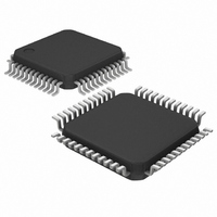
MAX9248ECM/V+ Maxim Integrated Products, MAX9248ECM/V+ Datasheet - Page 7

MAX9248ECM/V+
Manufacturer Part Number
MAX9248ECM/V+
Description
IC DESERIALIZER LVDS 48-LQFP
Manufacturer
Maxim Integrated Products
Datasheet
1.MAX9250ECMT.pdf
(20 pages)
Specifications of MAX9248ECM/V+
Function
Deserializer
Data Rate
840Mbps
Input Type
LVDS
Output Type
LVTTL, LVCMOS
Number Of Inputs
1
Number Of Outputs
18
Voltage - Supply
3 V ~ 3.6 V
Operating Temperature
-40°C ~ 85°C
Mounting Type
Surface Mount
Package / Case
48-LQFP
Lead Free Status / RoHS Status
Lead free / RoHS Compliant
MAX9248 MAX9250
25, 37
26, 38
15–23
10
11
12
13
14
24
1
2
3
4
5
6
7
8
9
PIN
25, 37
26, 38
15–23
10
11
12
13
24
—
1
2
3
4
5
6
7
8
9
_______________________________________________________________________________________
CNTL_OUT0–
CNTL_OUT8
LVDSGND
PWRDWN
V
V
PLLGND
DE_OUT
REFCLK
V
CCOGND
NAME
CCLVDS
RNG1
RNG0
V
GND
CCPLL
V
IN+
R/F
IN-
CCO
SS
CC
Rising or Falling Latch Edge Select. LVTTL/LVCMOS input. Selects the edge of PCLK_OUT
for latching data into the next chip. Set R/F = high for a rising latch edge. Set R/F = low for a
falling latch edge. Internally pulled down to GND.
LVTTL/LVCMOS Range Select Input. Set to the range that includes the serializer parallel
clock input frequency. Internally pulled down to GND.
LV D S S up p l y V ol tag e. Byp ass to LV D S G N D w i th 0.1µF and 0.001µF cap aci tor s i n p ar al l el as
cl ose to the d evi ce as p ossi b l e, w i th the sm al l est val ue cap aci tor cl osest to the sup p l y p i n.
Noninverting LVDS Serial-Data Input
Inverting LVDS Serial-Data Input
LVDS Supply Ground
PLL Supply Ground
PLL Supply Voltage. Bypass to PLLGND with 0.1µF and 0.001µF capacitors in parallel as
close to the device as possible with the smallest value capacitor closest to the supply pin.
LVTTL/LVCMOS Range Select Input. Set to the range that includes the serializer parallel
clock input frequency. Internal pulldown to GND.
Digital Supply Ground
Digital Supply Voltage. Supply for LVTTL/LVCMOS inputs and digital circuits. Bypass to
GND with 0.1µF and 0.001µF capacitors in parallel as close to the device as possible with
the smallest value capacitor closest to the supply pin.
LVTTL/LVCMOS Reference Clock Input. Apply a reference clock that is within ±2% of the
serializer PCLK_IN frequency. Internally pulled down to GND.
LVTTL/LVCMOS Power-Down Input. Internally pulled down to GND.
LV TTL/LV C M OS S p r ead - S p ectr um Inp ut. S S sel ects the fr eq uency sp r ead of P C LK_O U T and
outp ut d ata r el ati ve to P C LK_IN . D r i ve S S hi g h for 4% sp r ead and p ul l l ow for 2% sp r ead .
LVTTL/LVCMOS Control Data Outputs. CNTL_OUT[8:0] are latched into the next chip on the
rising or falling edge of PCLK_OUT as selected by R/F when DE_OUT is low, and are held
at the last state when DE_OUT is high.
LVTTL/LVCMOS Data-Enable Output. High indicates RGB_OUT[17:0] are active. Low
indicates CNTL_OUT[8:0] are active.
Output Supply Ground
Output Supply Voltage. Bypass to GND with 0.1µF and 0.001µF capacitors in parallel as
close to the device as possible with the smallest value capacitor closest to the supply pin.
DC-Balanced LVDS Deserializers
27-Bit, 2.5MHz to 42MHz
FUNCTION
Pin Description
7


