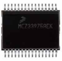
MCZ33975AEK Freescale Semiconductor, MCZ33975AEK Datasheet - Page 25

MCZ33975AEK
Manufacturer Part Number
MCZ33975AEK
Description
IC MULTIPLE SWITCH DETECT 32SOIC
Manufacturer
Freescale Semiconductor
Datasheet
1.MCZ33975AEK.pdf
(34 pages)
Specifications of MCZ33975AEK
Applications
Automotive
Interface
SPI
Voltage - Supply
5.5 V ~ 28 V
Package / Case
32-SOIC (7.5mm Width) Exposed Pad, 32-eSOIC, 32-HSOIC
Mounting Type
Surface Mount
Lead Free Status / RoHS Status
Lead free / RoHS Compliant
grounded and brought back to the module ground, as
illustrated in
impedance of the sensor, the analog voltage on the input will
represent the position of the sensor.
current to an analog sensor may induce error due to the
accuracy of the current source. For this reason, a ratiometric
conversion must be considered. Using two current sources
(one for the sensor and one to set the reference voltage to the
A/D converter) will yield a maximum error (owing to the
33975) of 4%.
calibration. In this example, we use the resistor values from
Figure 14
other. The user may use the module end-of-line tester to
calculate the error in the A/D conversion. By placing a 1.0kΩ,
0.1% resistor in the end-of-line test equipment and assuming
a perfect 4.0mA current source from the 33975, a calculated
A/D conversion may be obtained.
Analog Integrated Circuit Device Data
Freescale Semiconductor
To read a potentiometer sensor, the wiper should be
Using the Analog feature to provide 4.0mA of pull-up
Higher accuracy may be achieved through module level
VBAT
VBAT
Analog Sensor
or Analog Switch
R
4.0mA
1
I
1
Figure 14. Analog Ratiometric Conversion
and assume the current sources are 4% from each
ADC =
SG12
SG13
Figure
SG0
SG1
SP0
SP1
SP7
4.0mA
I
2
ADC =
32
mA
mA
32
1.21kΩ
ADC = 210 counts
0.1%
4.0mA x 1.21kΩ
V
V
14. With the wiper changing the
4.0mA x 1.0kΩ
PWR
PWR
33975
V
4.36V to 5.32V
V
I1 x R1
I2 x R2
PWR
PWR
4.0
mA
4.0
mA
R
2
WAKE
AMUX
VPWR
SCLK
x 255
VDD
INT
CS
SO
SI
x 255
V
DD
MOSI
SCLK
CS
MISO
INT
V
V
AN0
Analog
REF(H)
REF(L)
MCU
Ports
(neglecting the resistor tolerance and AMUX input offset
voltage). Now calculate the count value induced by the
mismatch in current sources. From a sample device the
maximum current source was measured at 3.979mA and
minimum current source was measured at 3.933mA. This
yields 1.16% error in A/D conversion due to the current
source mismatch. The A/D measurement will be as follows:
correction factor of 1.0115 may be used to correct the value:
memory and used in the A/D calculation for the specific input.
Each input used as analog measurement will have a
dedicated calibrated error correction factor.
POWER MOSFET/LED DRIVER AND MONITOR
it may be used to drive small loads like LEDs or MOSFET
gates. It was specifically designed to power up in the Normal
Mode with the inputs tri-state. This was done to ensure the
LEDs or MOSFETs connected to the 33975 power up in the
off-state. The Switch Programmable (SP0–SP7) inputs have
a source-and-sink capability, providing effective MOSFET
gate control. To complete the circuit, a pull-down resistor
should be used to keep the gate from floating during the
Sleep Modes.
where the SG0 input is used to monitor the drain-to-source
voltage of the external MOSFET. The 750Ω resistor is used
to set the drain-to-source trip voltage. With the 4.0mA current
source enabled, an interrupt will be generated when the
drain-to-source voltage is approximately 1.0V.
Using the equation yields the following:
The ADC value of 213 counts is the value with 0% error
This A/D conversion is 1.16% low in value. The error
An error correction factor may then be stored in E
Because of the flexible programming of the 33975 device,
ADC =
Figure
ADC = 208 counts x 1.0116
3.979 mA x 1.21kΩ
ADC = 210 counts
15, page 26, shows an application
3.933 mA x 1.0kΩ
ADC = 208 counts
TYPICAL APPLICATIONS
OPERATIONAL MODES
x 255
2
33975
25


