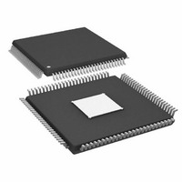
AD8159ASVZ Analog Devices Inc, AD8159ASVZ Datasheet - Page 20

AD8159ASVZ
Manufacturer Part Number
AD8159ASVZ
Description
IC MUX/DEMUX QUAD BUFF 100TQFP
Manufacturer
Analog Devices Inc
Series
XStream™r
Datasheet
1.AD8159ASVZ.pdf
(24 pages)
Specifications of AD8159ASVZ
Applications
2:1 Multiplexer/1:2 De-Multiplexer
Interface
Serial
Voltage - Supply
3 V ~ 3.6 V
Package / Case
100-TQFP Exposed Pad, 100-eTQFP, 100-HTQFP, 100-VQFP
Mounting Type
Surface Mount
Crosspoint Switch Type
Digital
Input / Output Configuration
LVPECL, CML / CML
Control Interface
Parallel
Supply Voltage Range
3V To 3.6V
Operating Temperature Range
-40°C To +85°C
Lead Free Status / RoHS Status
Lead free / RoHS Compliant
Available stocks
Company
Part Number
Manufacturer
Quantity
Price
Company:
Part Number:
AD8159ASVZ
Manufacturer:
Analog Devices Inc
Quantity:
135
Company:
Part Number:
AD8159ASVZ
Manufacturer:
AnalogDevices
Quantity:
321
Company:
Part Number:
AD8159ASVZ
Manufacturer:
ADI
Quantity:
174
Company:
Part Number:
AD8159ASVZ
Manufacturer:
Analog Devices Inc
Quantity:
10 000
Part Number:
AD8159ASVZ
Manufacturer:
ADI/亚德诺
Quantity:
20 000
AD8159
Consider the following example: a driver dc-coupled to the
input of the AD8159. The AD8159 input termination voltage
(V
set to the same level; that is, V
differential swing is desired, the total output current of the driver
is 16 mA. At balance, the output current is divided evenly between
the two sides of the differential signal path, 8 mA to each side.
This 8 mA of current flows through the parallel combination of the
55 Ω input termination resistor on the AD8159 and the 50 Ω
output termination resistor on the driver, resulting in a common-
mode level of
The user can then use Figure 25 to determine the allowable
range of values for V
based on an 800 mV p-p differential swing.
Table 9. Output Voltage Levels for Port A and Port B
PE Setting
0
1
2
3
Table 10. Output Voltage Levels for Port C
PE Setting
0
1
2
3
Table 11. Symbol Definitions
Symbol
V
V
V
V
V
V
OSE-DC
OSE-BOOST
OCM
OCM
H
L
TTI
) and the driver output termination voltage (V
V
(dc-coupled)
(ac-coupled)
TTI
− 8 mA × (50 Ω || 55 Ω) = V
I
16
20
24
28
I
20
24
28
32
T
T
(mA)
(mA)
TTI
that meets the input compliance range
V
400
400
400
400
V
400
400
400
400
TTI
OSE-DC
OSE-DC
= V
Formula
I
V
V
V
V
I
T
T
TTO
TTO
OCM
OCM
× 25 Ω
TTOD
(mV p-p)
(mV p-p)
PE
=
– I
– I
TTI
+ V
− V
0
= 3.3 V. If an 800 mV p-p
× 25 Ω
T
T
/2 × 25 Ω
/2 × 50 Ω
− 210 mV
OSE-BOOST
OSE-BOOST
/2
/2
TTOD
V
400
500
600
700
V
400
500
600
700
OSE-BOOST
OSE-BOOST
) are both
(mV p-p)
(mV p-p)
Rev. B | Page 20 of 24
OUTPUT COMPLIANCE
Figure 43 is depicts the single-ended waveform at the output of
the AD8159. The common-mode level (V
(V
current (I
topology of the far-end receiver, and whether ac coupling or dc
coupling is used. Keep in mind that the output tail current varies
with the pre-emphasis level. The user must ensure that the high
(V
single-ended absolute voltage range limits as specified in Table 1.
Failure to understand the implications of output signal levels
and the choice of ac coupling or dc coupling may lead to transistor
saturation and poor transmitter performance.
Table 9 and Table 10 show the typical output levels for Port A/
Port B and Port C, respectively, where V
50 Ω far-end terminations to a 3.3 V supply.
V
V
OCM
TTO
V
3.1
3.05
3
2.95
V
3.05
3
2.95
2.9
Definition
Single-ended output voltage swing after settling
Boosted single-ended output voltage swing
Common-mode voltage when the output is dc-coupled
Common-mode voltage when the output is ac-coupled
High single-ended output voltage excursion
Low single-ended output voltage excursion
OSE-BOOST
H
OCM
OCM
) and low (V
(V)
(V)
T
) of this waveform are a function of the output tail
DC-Coupled
DC-Coupled
), the output termination supply voltage (V
~320ps
V
3.3
3.3
3.3
3.3
V
3.25
3.25
3.25
3.25
Figure 43. Single-Ended Output Waveform
H
H
L
) voltage excursions at the output are within the
(V)
(V)
V
2.9
2.8
2.7
2.6
V
2.85
2.75
2.65
2.55
L
L
(V)
(V)
V
2.9
2.8
2.7
2.6
V
2.8
2.7
2.6
2.5
OCM
OCM
(V)
(V)
OCM
CC
= V
) and the amplitude
AC-Coupled
AC-Coupled
V
OSE-DC
TTO
V
3.1
3.05
3
2.95
V
3
2.95
2.9
2.85
H
H
(V)
= 3.3 V, with
(V)
V
TTO
OSE-BOOST
), the
V
2.7
2.55
2.4
2.25
V
2.6
2.45
2.3
2.15
L
L
(V)
(V)
V
V
H
L


