HCTL-2032-SC Avago Technologies US Inc., HCTL-2032-SC Datasheet - Page 16
HCTL-2032-SC
Manufacturer Part Number
HCTL-2032-SC
Description
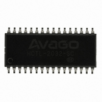
IC DECODER/COUNTER 32BIT 32-SOIC
Manufacturer
Avago Technologies US Inc.
Type
Quadrature Decoder/Counter Interface ICr
Datasheet
1.HCTL-2032-SC.pdf
(21 pages)
Specifications of HCTL-2032-SC
Package / Case
32-SOIC (7.5mm Width)
Applications
Encoder to Microprocessor
Interface
8-Bit Tristate
Voltage - Supply
4.5 V ~ 5.5 V
Mounting Type
Surface Mount
Maximum Operating Temperature
+ 100 C
Minimum Operating Temperature
- 40 C
Mounting Style
SMD/SMT
Lead Free Status / RoHS Status
Lead free / RoHS Compliant
Lead Free Status / RoHS Status
Lead free / RoHS Compliant, Lead free / RoHS Compliant
Other names
516-1885-5
HCTL-2032-SC
HCTL-2032-SC
Available stocks
Company
Part Number
Manufacturer
Quantity
Price
Company:

Part Number:
HCTL-2032-SC
Manufacturer:
AVX
Quantity:
24 000
Part Number:
HCTL-2032-SC
Manufacturer:
AGILENT
Quantity:
20 000


Position Data Latch
The position data latch is a 32-bit latch which captures
the position counter output data on each rising clock
edge, except when its inputs are disabled by the inhibit
logic section during four-byte read operations. The out-
put data is passed to the bus interface section. When ac-
tive, a signal from the inhibit logic section prevents new
data from being captured by the latch, keeping the data
stable while successive reads are made through the bus
section. The latch is automatically re-enabled at the end
of these reads. The latch is cleared to 0 asynchronously by
the RST signal.
Inhibit Logic
The Inhibit Logic Section samples the OE, SEL1 and SEL2
signals on the falling edge of the clock and, in response
to certain conditions (see Figure 15), inhibits the position
data latch. The RST signal asynchronously clears the in-
hibit logic, enabling the latch.
Bus Interface
The bus interface section consists of a 32 to 8 line multi-
plexer and an 8-bit, three-state output buffer. The mul-
tiplexer allows independent access to the low and high
bytes of the position data latch. The SEL1, SEL2 and OE
signals determine which byte is output and whether or
not the output bus is in the high-Z state. In the HCTL-
20XX-XX, the data latch is 32 bit wide.
Figure 15. Four Bytes Read Sequence
Step
3
4
SEL1
H
H
X
L
L
SEL2
H
H
L
L
X
OE
H
L
L
L
L
CLK
Quadrature Decoder Output
The quadrature decoder output section consists of count
and up/down outputs derived from the 4x/2x/1x decod-
er mode of the HCTL-2032 / 2032-SC. When the decoder
has detected a count, a pulse, one-half clock cycle long,
will be output on the CNT
cur during the clock cycle in which the internal counter
is updated. The U/D pin will be set to the proper voltage
level one clock cycle before the rising edge of the CNT-
DCDR
of the CNT
the inhibit logic.
Cascade Output
The cascade output also consists of count and up/down
outputs. When the HCTL-2032 / 2032-SC internal coun-
ter overflows or underflows, a pulse, one-half clock cycle
long, will be output on the CNT
occur during the clock cycle in which the internal coun-
ter is updated. The U/D pin will be set to the proper volt-
age level one clock cycle before the rising edge of the
CNT
edge of the CNT
by the inhibit logic.
CAS
pulse, and held one clock cycle after the rising edge
Inhibit Signal
pulse, and held one clock cycle after the rising
0
DCDR
(HCTL-2032 / 2032-SC only)
pulse. These outputs are not affected by
CAS
pulse. These outputs are not affected
Action
Set inhibit; Read MSB
Read
Read 3
Read LSB
Completes inhibit logic reset
nd
(HCTL-2032 / 2032-SC only)
DCDR
rd
Byte
Byte
pin. This output will oc-
CAS
pin. This output will
Related parts for HCTL-2032-SC
Image
Part Number
Description
Manufacturer
Datasheet
Request
R

Part Number:
Description:
IC DECODER/COUNTER 16BIT 20-PLCC
Manufacturer:
Avago Technologies US Inc.
Datasheet:

Part Number:
Description:
IC,Servo Encoder,CMOS,DIP,20PIN,PLASTIC
Manufacturer:
Avago Technologies US Inc.
Datasheet:

Part Number:
Description:
Quadrature Decoder/Counter Interface IC 16-Pin PDIP
Manufacturer:
Avago Technologies US Inc.
Datasheet:

Part Number:
Description:
QUADRATURE DECODER/COUNTER INTER
Manufacturer:
Avago Technologies US Inc.
Datasheet:

Part Number:
Description:
IC MOTION CONTROL GP 40DIP
Manufacturer:
Avago Technologies US Inc.
Datasheet:

Part Number:
Description:
Motion Control IC, PLCC
Manufacturer:
Avago Technologies US Inc.

Part Number:
Description:
Fiber Optic Transmitters, Receivers, Transceivers Quadrature Decoder
Manufacturer:
Avago Technologies US Inc.
Part Number:
Description:
IC MOTION CTRLR GP LP 40-DIP
Manufacturer:
Avago Technologies US Inc.
Datasheet:
Part Number:
Description:
IC MOTION CTRLR GP LP 44-PLCC
Manufacturer:
Avago Technologies US Inc.
Datasheet:

Part Number:
Description:
Manufacturer:
Agilent Technologies, Inc.
Datasheet:
Part Number:
Description:
Manufacturer:
Agilent Technologies, Inc.
Datasheet:

Part Number:
Description:
Manufacturer:
Avago Technologies
Datasheet:
Part Number:
Description:
Manufacturer:
Agilent Technologies, Inc.
Datasheet:
Part Number:
Description:
Manufacturer:
Agilent Technologies, Inc.
Datasheet:

Part Number:
Description:
IC DECODER/COUNTER 16BIT 16-DIP
Manufacturer:
Avago Technologies US Inc.
Datasheet: