RC28F320J3D75B Numonyx - A DIVISION OF MICRON SEMICONDUCTOR PRODUCTS, INC., RC28F320J3D75B Datasheet - Page 17
RC28F320J3D75B
Manufacturer Part Number
RC28F320J3D75B
Description
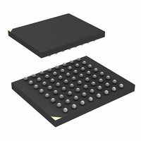
IC FLASH 32MBIT 75NS 64EZBGA
Manufacturer
Numonyx - A DIVISION OF MICRON SEMICONDUCTOR PRODUCTS, INC.
Series
-r
Datasheet
1.RC28F128J3D75B.pdf
(66 pages)
Specifications of RC28F320J3D75B
Format - Memory
FLASH
Memory Type
FLASH
Memory Size
32M (4Mx8, 2Mx16)
Speed
75ns
Interface
Parallel
Voltage - Supply
2.7 V ~ 3.6 V
Operating Temperature
-40°C ~ 85°C
Package / Case
64-EZBGA
Lead Free Status / Rohs Status
Contains lead / RoHS non-compliant
Other names
872859
872859TR
872859TR
RC28F320J3D75 S L8QS
RC28F320J3D75B
RC28F320J3D75BTR
872859TR
872859TR
RC28F320J3D75 S L8QS
RC28F320J3D75B
RC28F320J3D75BTR
Available stocks
Company
Part Number
Manufacturer
Quantity
Price
Company:

Part Number:
RC28F320J3D75B
Manufacturer:
Micron Technology Inc
Quantity:
10 000


Numonyx™ Embedded Flash Memory (J3 v D, Monolithic)
Table 3:
December 2007
316577-06
Symbol
D[15:8]
CE[2:0]
BYTE#
VCCQ
VPEN
WE#
OE#
GND
RP#
VCC
STS
RFU
NC
Signal Descriptions for Numonyx™ Embedded Flash Memory (J3 v D, Monolithic)
Open Drain
Output
Output
Supply
(Sheet 2 of 2)
Input/
Power
Power
Type
Input
Input
Input
Input
Input
Input
—
—
HIGH-BYTE DATA BUS: Inputs data during x16 buffer writes and programming operations.
Outputs array, CFI, or identifier data in the appropriate read mode; not used for Status Register
reads. Data is internally latched during write operations in x16 mode. D[15-8] float in x8 mode
CHIP ENABLE: Activate the 32-, 64-, 128-, and 256-Mbit devices’ control logic, input buffers,
decoders, and sense amplifiers. When the device is de-selected (see
Truth Table for 32-, 64-, 128- and 256-Mb” on page 31
levels.
All timing specifications are the same for these three signals. Device selection occurs with the first
edge of CE0, CE1, or CE2 that enables the device. Device deselection occurs with the first edge of
CE0, CE1, or CE2 that disables the device (see
32-, 64-, 128- and 256-Mb” on page 31
RESET: RP#-low resets internal automation and puts the device in power-down mode. RP#-high
enables normal operation. Exit from reset sets the device to read array mode. When driven low,
RP# inhibits write operations which provides data protection during power transitions.
OUTPUT ENABLE: Activates the device’s outputs through the data buffers during a read cycle.
OE# is active low.
WRITE ENABLE: Controls writes to the CUI, the Write Buffer, and array blocks. WE# is active low.
Addresses and data are latched on the rising edge of WE#.
STATUS: Indicates the status of the internal state machine. When configured in level mode
(default), it acts as a RY/BY# signal. When configured in one of its pulse modes, it can pulse to
indicate program and/or erase completion. For alternate configurations of the Status signal, see the
Configurations command and
to VCCQ with a pull-up resistor.
BYTE ENABLE: BYTE#-low places the device in x8 mode; data is input or output on D[7:0], while
D[15:8] is placed in High-Z. Address A0 selects between the high and low byte. BYTE#-high places
the device in x16 mode, and turns off the A0 input buffer. Address A1 becomes the lowest-order
address bit.
ERASE / PROGRAM / BLOCK LOCK ENABLE: For erasing array blocks, programming data, or
configuring lock-bits.
With V
CORE Power Supply: Core (logic) source voltage. Writes to the flash array are inhibited when V
≤ V
Caution: Device operation at invalid Vcc voltages should not be attempted.
I/O Power Supply: Power supply for Input/Output buffers.This ball can be tied directly to V
GROUND: Ground reference for device logic voltages. Connect to system ground.
No Connect: Lead is not internally connected; it may be driven or floated.
Reserved for Future Use: Balls designated as RFU are reserved by Numonyx for future device
functionality and enhancement.
lko
.
PEN
≤ V
PENLK
, memory contents cannot be altered.
Section 9.6, “Status Signal” on page 42
Name and Function
Table 16, “Chip Enable Truth Table for
).
Table 16, “Chip Enable
), power reduces to standby
. STS is to be tied
Datasheet
CC
.
CC
17
Related parts for RC28F320J3D75B
Image
Part Number
Description
Manufacturer
Datasheet
Request
R

Part Number:
Description:
IC FLASH 128MBIT 75NS 64EZBGA
Manufacturer:
Numonyx - A DIVISION OF MICRON SEMICONDUCTOR PRODUCTS, INC.
Datasheet:
Part Number:
Description:
IC FLASH 128MBIT 75NS 64EZBGA
Manufacturer:
Numonyx - A DIVISION OF MICRON SEMICONDUCTOR PRODUCTS, INC.
Datasheet:
Part Number:
Description:
IC FLASH 128MBIT 65NS 64EZBGA
Manufacturer:
Numonyx - A DIVISION OF MICRON SEMICONDUCTOR PRODUCTS, INC.
Datasheet:

Part Number:
Description:
IC FLASH 128MBIT 65NM 3V SO16
Manufacturer:
Numonyx - A DIVISION OF MICRON SEMICONDUCTOR PRODUCTS, INC.
Datasheet:
Part Number:
Description:
IC SRL FLASH 128MB NMX 24-BGAS
Manufacturer:
Numonyx - A DIVISION OF MICRON SEMICONDUCTOR PRODUCTS, INC.
Datasheet:
Part Number:
Description:
IC SRL FLASH 128MB NMX 24-BGA
Manufacturer:
Numonyx - A DIVISION OF MICRON SEMICONDUCTOR PRODUCTS, INC.
Datasheet:
Part Number:
Description:
IC SRL FLASH 128MB NMX 16-SOIC
Manufacturer:
Numonyx - A DIVISION OF MICRON SEMICONDUCTOR PRODUCTS, INC.
Datasheet:
Part Number:
Description:
IC SRL FLASH 128MB NMX 8-VDFPN
Manufacturer:
Numonyx - A DIVISION OF MICRON SEMICONDUCTOR PRODUCTS, INC.
Datasheet:
Part Number:
Description:
IC FLASH 128MBIT 75NS 64EZBGA
Manufacturer:
Numonyx - A DIVISION OF MICRON SEMICONDUCTOR PRODUCTS, INC.
Datasheet:
Part Number:
Description:
IC FLASH 128MBIT 75NS 64EZBGA
Manufacturer:
Numonyx - A DIVISION OF MICRON SEMICONDUCTOR PRODUCTS, INC.
Datasheet:
Part Number:
Description:
IC FLASH 32MBIT 75NS 64EZBGA
Manufacturer:
Numonyx - A DIVISION OF MICRON SEMICONDUCTOR PRODUCTS, INC.
Datasheet: