RC28F320J3D75B Numonyx - A DIVISION OF MICRON SEMICONDUCTOR PRODUCTS, INC., RC28F320J3D75B Datasheet - Page 19
RC28F320J3D75B
Manufacturer Part Number
RC28F320J3D75B
Description
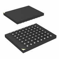
IC FLASH 32MBIT 75NS 64EZBGA
Manufacturer
Numonyx - A DIVISION OF MICRON SEMICONDUCTOR PRODUCTS, INC.
Series
-r
Datasheet
1.RC28F128J3D75B.pdf
(66 pages)
Specifications of RC28F320J3D75B
Format - Memory
FLASH
Memory Type
FLASH
Memory Size
32M (4Mx8, 2Mx16)
Speed
75ns
Interface
Parallel
Voltage - Supply
2.7 V ~ 3.6 V
Operating Temperature
-40°C ~ 85°C
Package / Case
64-EZBGA
Lead Free Status / Rohs Status
Contains lead / RoHS non-compliant
Other names
872859
872859TR
872859TR
RC28F320J3D75 S L8QS
RC28F320J3D75B
RC28F320J3D75BTR
872859TR
872859TR
RC28F320J3D75 S L8QS
RC28F320J3D75B
RC28F320J3D75BTR
Available stocks
Company
Part Number
Manufacturer
Quantity
Price
Company:

Part Number:
RC28F320J3D75B
Manufacturer:
Micron Technology Inc
Quantity:
10 000


Numonyx™ Embedded Flash Memory (J3 v D, Monolithic)
Table 6:
5.3.2
5.4
December 2007
316577-06
Power Supply
V
V
Voltage
V
CCQ(min)
PEN(min)
CC(min)
Power-Up/Down Sequence
† Power supplies connected or sequenced together.
Device inputs must not be driven until all supply voltages reach their minimum range.
RP# should be low during power transitions.
Power Supply Decoupling
When the device is enabled, many internal conditions change. Circuits are energized,
charge pumps are switched on, and internal voltage nodes are ramped. All of this
internal activities produce transient signals. The magnitude of the transient signals
depends on the device and system loading. To minimize the effect of these transient
signals, a 0.1 µF ceramic capacitor is required across each VCC/VSS and VCCQ signal.
Capacitors should be placed as close as possible to device connections.
Additionally, for every eight flash devices, a 4.7 µF electrolytic capacitor should be
placed between VCC and VSS at the power supply connection. This 4.7 µF capacitor
should help overcome voltage slumps caused by PCB trace inductance.
Reset
By holding the flash device in reset during power-up and power-down transitions,
invalid bus conditions may be masked. The flash device enters reset mode when RP# is
driven low. In reset, internal flash circuitry is disabled and outputs are placed in a high-
impedance state. After return from reset, a certain amount of time is required before
the flash device is able to perform normal operations. After return from reset, the flash
device defaults to asynchronous page mode. If RP# is driven low during a program or
erase operation, the program or erase operation will be aborted and the memory
contents at the aborted block or address are no longer valid. See
Waveform for Reset Operation” on page 29
timings.
2nd
1st
3rd
2nd
Power-UpSequence
1st
†
1st
2nd
†
Sequencing not
required
†
for detailed information regarding reset
2nd
3rd
1st
Power-Down Sequence
1st
2nd
†
Figure 14, “AC
2nd
1st
†
Sequencing not
required
Datasheet
†
19
Related parts for RC28F320J3D75B
Image
Part Number
Description
Manufacturer
Datasheet
Request
R

Part Number:
Description:
IC FLASH 128MBIT 75NS 64EZBGA
Manufacturer:
Numonyx - A DIVISION OF MICRON SEMICONDUCTOR PRODUCTS, INC.
Datasheet:
Part Number:
Description:
IC FLASH 128MBIT 75NS 64EZBGA
Manufacturer:
Numonyx - A DIVISION OF MICRON SEMICONDUCTOR PRODUCTS, INC.
Datasheet:
Part Number:
Description:
IC FLASH 128MBIT 65NS 64EZBGA
Manufacturer:
Numonyx - A DIVISION OF MICRON SEMICONDUCTOR PRODUCTS, INC.
Datasheet:

Part Number:
Description:
IC FLASH 128MBIT 65NM 3V SO16
Manufacturer:
Numonyx - A DIVISION OF MICRON SEMICONDUCTOR PRODUCTS, INC.
Datasheet:
Part Number:
Description:
IC SRL FLASH 128MB NMX 24-BGAS
Manufacturer:
Numonyx - A DIVISION OF MICRON SEMICONDUCTOR PRODUCTS, INC.
Datasheet:
Part Number:
Description:
IC SRL FLASH 128MB NMX 24-BGA
Manufacturer:
Numonyx - A DIVISION OF MICRON SEMICONDUCTOR PRODUCTS, INC.
Datasheet:
Part Number:
Description:
IC SRL FLASH 128MB NMX 16-SOIC
Manufacturer:
Numonyx - A DIVISION OF MICRON SEMICONDUCTOR PRODUCTS, INC.
Datasheet:
Part Number:
Description:
IC SRL FLASH 128MB NMX 8-VDFPN
Manufacturer:
Numonyx - A DIVISION OF MICRON SEMICONDUCTOR PRODUCTS, INC.
Datasheet:
Part Number:
Description:
IC FLASH 128MBIT 75NS 64EZBGA
Manufacturer:
Numonyx - A DIVISION OF MICRON SEMICONDUCTOR PRODUCTS, INC.
Datasheet:
Part Number:
Description:
IC FLASH 128MBIT 75NS 64EZBGA
Manufacturer:
Numonyx - A DIVISION OF MICRON SEMICONDUCTOR PRODUCTS, INC.
Datasheet:
Part Number:
Description:
IC FLASH 32MBIT 75NS 64EZBGA
Manufacturer:
Numonyx - A DIVISION OF MICRON SEMICONDUCTOR PRODUCTS, INC.
Datasheet: