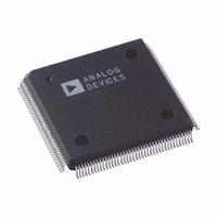
AD9887AKS-140 Analog Devices Inc, AD9887AKS-140 Datasheet - Page 31

AD9887AKS-140
Manufacturer Part Number
AD9887AKS-140
Description
IC INTRFACE ANALOG/DVI 160-MQFP
Manufacturer
Analog Devices Inc
Datasheet
1.AD9887AKSZ-100.pdf
(40 pages)
Specifications of AD9887AKS-140
Rohs Status
RoHS non-compliant
Applications
Graphic Cards, VGA Interfaces
Interface
Analog and Digital
Voltage - Supply
3.15 V ~ 3.45 V
Package / Case
160-MQFP, 160-PQFP
Mounting Type
Surface Mount
Available stocks
Company
Part Number
Manufacturer
Quantity
Price
Company:
Part Number:
AD9887AKS-140
Manufacturer:
AD
Quantity:
275
Company:
Part Number:
AD9887AKS-140
Manufacturer:
TOS
Quantity:
160
Company:
Part Number:
AD9887AKS-140
Manufacturer:
AD
Quantity:
586
Part Number:
AD9887AKS-140
Manufacturer:
ADI/亚德诺
Quantity:
20 000
0E
0E
0F
0F
When DEMUX = 0, this bit is ignored as data always
comes out of only Port A.
4 HSYNC Output Polarity
One bit that determines the polarity of the HSYNC out-
put and the SOG output. Table XV shows the effect of
this option. SYNC indicates the logic state of the sync pulse.
Table XV. HSYNC Output Polarity Settings
Setting
0
1
The default setting for this register is 1. (This option
works on both the analog and digital interfaces.)
3 VSYNC Output Invert
One bit that inverts the polarity of the VSYNC output.
Table XVI shows the effect of this option.
Table XVI. VSYNC Output Polarity Settings
Setting
0
1
The default setting for this register is 1. (This option
works on both the analog and digital interfaces.)
7 HSYNC Input Polarity
A bit that must be set to indicate the polarity of the HSYNC
signal that is applied to the PLL HSYNC input.
Table XVII. HSYNC Input Polarity Settings
HSPOL
0
1
Active LOW is the traditional negative-going Hsync pulse.
All timing is based on the leading edge of Hsync, which is
the FALLING edge. The rising edge has no effect.
Active HIGH is inverted from the traditional Hsync, with a
positive-going pulse. This means that timing will be based on
the leading edge of Hsync, which is now the RISING edge.
The device will operate if this bit is set incorrectly, but the
internally generated clamp position, as established by
CLPOS, will not be placed as expected, which may gener-
ate clamping errors.
The power-up default value is HSPOL = 1.
6 COAST Input Polarity
A bit to indicate the polarity of the COAST signal that is
applied to the PLL COAST input.
Table XVIII. COAST Input Polarity Settings
CSTPOL
0
1
SYNC
Logic 1 (Positive Polarity)
Logic 0 (Negative Polarity)
VSYNC Output
Invert
No Invert
Function
Active LOW
Active HIGH
Function
Active LOW
Active HIGH
0F
0F
0F
Active LOW means that the clock generator will ignore Hsync
inputs when COAST is LOW, and continue operating at the
same nominal frequency until COAST goes HIGH.
Active HIGH means that the clock generator will ignore
Hsync inputs when COAST is HIGH, and continue operat-
ing at the same nominal frequency until COAST goes LOW.
This function needs to be used along with the COAST
polarity override bit (Register 14, Bit 1).
The power-up default value is CSTPOL = 1.
5 Clamp Input Signal Source
A bit that determines the source of clamp timing.
EXTCLMP
0
1
A 0 enables the clamp timing circuitry controlled by
CLPLACE and CLDUR. The clamp position and dura-
tion is counted from the leading edge of Hsync.
A 1 enables the external CLAMP input pin. The three
channels are clamped when the CLAMP signal is
active. The polarity of CLAMP is determined by the
CLAMPOL bit.
The power-up default value is EXTCLMP = 0.
4 CLAMP Input Signal Polarity
A bit that determines the polarity of the externally pro-
vided CLAMP signal.
Table XX. CLAMP Input Signal Polarity Settings
EXTCLMP
0
1
A Logic 0 means that the circuit will clamp when CLAMP
is HIGH, and it will pass the signal to the ADC when
CLAMP is LOW.
A Logic 1 means that the circuit will clamp when CLAMP
is LOW, and it will pass the signal to the ADC when
CLAMP is HIGH.
The power-up default value is CLAMPOL = 1.
3 External Clock Select
A bit that determines the source of the pixel clock.
EXTCLK
0
1
A Logic 0 enables the internal PLL that generates the
pixel clock from an externally provided Hsync.
Table XIX. Clamp Input Signal Source Settings
Table XXI. External Clock Select Settings
Function
Internally-Generated Clamp
Externally-Provided Clamp Signal
Function
Active LOW
Active HIGH
Function
Internally Generated Clock
Externally Provided Clock Signal
AD9887


