XCARD XC-1 XMOS, XCARD XC-1 Datasheet - Page 13
XCARD XC-1
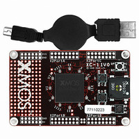
Manufacturer Part Number
XCARD XC-1
Description
BOARD DEV KIT XS1-G4
Manufacturer
XMOS
Series
XCore™r
Type
MCUr
Datasheets
1.XS1-G04B-FB144-C4.pdf
(22 pages)
2.XCARD_XC-1.pdf
(2 pages)
3.XCARD_XC-1.pdf
(21 pages)
4.XCARD_XC-1.pdf
(17 pages)
Specifications of XCARD XC-1
Contents
Board, Cable
Lead Free Status / Rohs Status
Lead free / RoHS Compliant
For Use With/related Products
XS1-G4
Other names
880-1013


XS1-G4 144BGA Datasheet (3.5)
To ensure correct device operation, the VDDIO and OTP_VDDIO supplies should be
3.3 ESD Stress Voltage
3.4 Reset Timing
User code must wait for the device to reset, the PLL to be locked and system code to
be started, before it can be run.
3.5 Power Supply
Power is applied to the device through the IO_VDD and VDD balls. Several balls of
each type are provided to minimize the effect of inductance within the package. All
supply pins must be connected. Each supply should be decoupled close to the chip
by several 100nF low inductance (for example, ceramic) capacitors between IO_VDD
and GND, and VDD and GND.
Input voltages must not exceed specification with respect to IO_VDD, VDD and GND,
even during power up and power down ramping. Permanent damage can occur if the
operation exceeds these ranges.
3.5.1 Power Supply Sequencing
present before the VDD supply. Specifically, the VDDIO and OTP_VDDIO supplies
should rise to their nominal operating range with VDD held at 0V. The VDD supply
should then rise to its nominal operating range with a rise time of less than 10ms.
ESD Model
HBM
MM
Parameters
Reset pulse width for correct start-up
PLL Lock
ISA (BOOT)
2. Voltages with respect to IO VSS
3. Internal pull-up resistors are fitted to general purpose XCore I/O pins. Applies to both
4. Use for unused I/O only—the internal pull up resistor is not recommended as a
XCore I/O and XCore link I/Os.
substitute for an external pull-up resistor.
ESD Stress Voltage
2.0 KV
200 V
www.xmos.com
MIN
100
TYP
MAX
1
100
UNITS
ns
ms
s
Notes
Notes
13/22
Related parts for XCARD XC-1
Image
Part Number
Description
Manufacturer
Datasheet
Request
R

Part Number:
Description:
BOARD DEV KIT XS1-G4 ETHERNET
Manufacturer:
XMOS
Datasheet:

Part Number:
Description:
BOARD DEV KIT XS1-G4
Manufacturer:
XMOS
Datasheet:

Part Number:
Description:
DEV KIT EVENT-DRIVEN PROC XS1-L1
Manufacturer:
XMOS
Datasheet:

Part Number:
Description:
BOARD KIT XS1-G4 LED CTRL TILE
Manufacturer:
XMOS
Datasheet:

Part Number:
Description:
ADAPTER USB DEBUGGER JTAG XSYS2
Manufacturer:
XMOS
Datasheet:

Part Number:
Description:
IC MPU 32BIT SINGLE CORE 64LQFP
Manufacturer:
XMOS
Datasheet:

Part Number:
Description:
IC MPU 32BIT SINGLE CORE 64LQFP
Manufacturer:
XMOS
Datasheet:
Part Number:
Description:
IC MPU 32BIT SINGLE CORE 64LQFP
Manufacturer:
XMOS
Datasheet:

Part Number:
Description:
IC MPU 32BIT SINGLE CORE 64LQFP
Manufacturer:
XMOS
Datasheet:
Part Number:
Description:
IC MPU 32BIT SINGLE CORE 64LQFP
Manufacturer:
XMOS
Datasheet:

Part Number:
Description:
IC MPU 32BIT SINGLE CORE 128TQFP
Manufacturer:
XMOS
Datasheet:
Part Number:
Description:
IC MPU 32BIT SINGLE CORE 64LQFP
Manufacturer:
XMOS
Datasheet:
Part Number:
Description:
IC MPU 32BIT SINGLE CORE 128TQFP
Manufacturer:
XMOS
Datasheet:
Part Number:
Description:
IC MPU 32BIT SINGLE CORE 128TQFP
Manufacturer:
XMOS
Datasheet:

Part Number:
Description:
IC MPU 32BIT DUAL CORE 124QFN
Manufacturer:
XMOS
Datasheet: