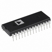
ADG406BNZ Analog Devices Inc, ADG406BNZ Datasheet - Page 4

ADG406BNZ
Manufacturer Part Number
ADG406BNZ
Description
IC MULTIPLEXER 16X1 28DIP
Manufacturer
Analog Devices Inc
Series
LC²MOSr
Datasheet
1.ADG406BNZ.pdf
(20 pages)
Specifications of ADG406BNZ
Function
Multiplexer
Circuit
1 x 16:1
On-state Resistance
80 Ohm
Voltage Supply Source
Single Supply
Voltage - Supply, Single/dual (±)
5V, 12V
Current - Supply
100µA
Operating Temperature
-40°C ~ 85°C
Mounting Type
Through Hole
Package / Case
28-DIP (0.600", 15.24mm)
No. Of Circuits
1
Supply Current
100µA
On State Resistance Max
50ohm
Supply Voltage Range
10.8V To 13.2V, ± 13.5V To ± 16.5V
Operating Temperature Range
-40°C To +85°C
Lead Free Status / RoHS Status
Lead free / RoHS Compliant
Available stocks
Company
Part Number
Manufacturer
Quantity
Price
Part Number:
ADG406BNZ
Manufacturer:
ADI/亚德诺
Quantity:
20 000
ADG406/ADG407/ADG426
SPECIFICATIONS
DUAL SUPPLY
V
Table 1.
Parameter
ANALOG SWITCH
LEAKAGE CURRENTS
DIGITAL INPUTS
DYNAMIC CHARACTERISTICS
DD
Analog Signal Range
R
R
Source Off Leakage I
Drain Off Leakage I
Channel On Leakage I
Input High Voltage, V
Input Low Voltage, V
Input Current
C
t
Break Before Make Delay, t
t
t
ADG426 Only
Charge Injection
Off Isolation
Channel-to-Channel Crosstalk
C
C
C
TRANSITION
ON
OFF
ON
ON
IN
S
D
D
= +15 V ± 10%, V
, C
ADG406, ADG426
ADG407
ADG406, ADG426
ADG407
I
t
t
t
t
ADG406, ADG426
ADG407
ADG406, ADG426
ADG407
(Off )
, Digital Input Capacitance
INL
(Off )
(EN, WR)
W
S
H
RS
Match
(EN, RS)
, Address, Enable Setup Time
, Address, Enable Hold Time
, Write Pulse Width
, Reset Pulse Width
S
or I
(On)
INH
1
D
S
SS
INL
(Off)
(Off )
D
INH
, I
= −15 V ± 10%, GND = 0 V, unless otherwise noted.
S
(On)
OPEN
2
+25°C
50
80
4
±0.5
±1
±1
±1
±1
8
120
150
10
120
160
110
150
8
−75
85
5
50
25
60
40
−40°C to +85°C
125
±20
±20
±20
±20
±20
2.4
0.8
±1
250
10
175
225
130
180
100
100
10
100
V
SS
to V
DD
Rev. B | Page 4 of 20
Unit
V
Ω typ
Ω max
Ω typ
nA max
nA max
nA max
nA max
nA max
V min
V max
μA max
pF typ
ns typ
ns max
ns min
ns typ
ns max
ns typ
ns max
ns min
ns min
ns min
ns min
pC typ
dB typ
dB typ
pF typ
pF typ
pF typ
pF typ
pF typ
Test Conditions/Comments
V
V
V
V
V
V
V
V
f = 1 MHz
R
R
R
R
V
V
See Figure 34
R
V
R
f = 1 MHz
f = 1 MHz
f = 1 MHz
D
DD
D
DD
D
D
S
IN
L
L
L
L
S
S
L
EN
L
= 300 Ω, C
= 1 k Ω, f = 100 kHz;
= V
= 300 Ω, C
= 300 Ω, C
= 300 Ω, C
= +5 V
= 0 V, R
= 1 k Ω, f = 100 kHz, see Figure 36
= ±10 V, I
= 0 V, I
= ±10 V, V
= ±10 V, V
= 0 or V
= 0 V, see Figure 35
= +13.5 V, V
= +16.5 V, V
D
= ±10 V; see Figure 28
S
S
= −1 mA
DD
= 0 Ω, C
S
L
S
S
L
L
L
= −1 mA
= 35 pF; V
= +10 V, see Figure 26
= +10 V; see Figure 27
= 35 pF; V
= 35 pF; V
= 35 pF; V
SS
SS
= −13.5 V
= −16.5 V
L
= 1 nF;
S
= +5 V, see Figure 30
1
S
S
= ±10 V, V
= 5 V, see Figure 31
= 5 V, see Figure 31
2
= +10 V; see Figure 29


