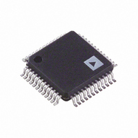
ADG726BSUZ Analog Devices Inc, ADG726BSUZ Datasheet - Page 3
ADG726BSUZ
Manufacturer Part Number
ADG726BSUZ
Description
IC MULTIPLEXER DUAL 16X1 48TQFP
Manufacturer
Analog Devices Inc
Datasheet
1.ADG732BSUZ.pdf
(12 pages)
Specifications of ADG726BSUZ
Function
Multiplexer
Circuit
2 x 16:1
On-state Resistance
5.5 Ohm
Voltage Supply Source
Single, Dual Supply
Voltage - Supply, Single/dual (±)
1.8 V ~ 5.5 V, ±2.5 V
Current - Supply
10µA
Operating Temperature
-40°C ~ 85°C
Mounting Type
Surface Mount
Package / Case
48-TQFP, 48-VQFP
No. Of Circuits
2
Supply Current
10µA
On State Resistance Max
4ohm
Supply Voltage Range
1.8V To 5.5V
Operating Temperature Range
-40°C To +85°C
Analog Switch Case Style
TQFP
Lead Free Status / RoHS Status
Lead free / RoHS Compliant
Available stocks
Company
Part Number
Manufacturer
Quantity
Price
Company:

Part Number:
ADG726BSUZ
Manufacturer:
Analog Devices Inc
Quantity:
1 818
Company:
Part Number:
ADG726BSUZ
Manufacturer:
Analog Devices Inc
Quantity:
10 000
Part Number:
ADG726BSUZ
Manufacturer:
ADI/亚德诺
Quantity:
20 000
Company:
Part Number:
ADG726BSUZ-REEL
Manufacturer:
Analog Devices Inc
Quantity:
10 000


SPECIFICATIONS
Parameter
LEAKAGE CURRENTS
DIGITAL INPUTS
DYNAMIC CHARACTERISTICS
POWER REQUIREMENTS
I
NOTES
1
2
Specifications subject to change without notice.
REV. 0
ANALOG SWITCH
DD
Temperature ranges are as follows: B Version: –40°C to +85°C.
Guaranteed by design; not subject to production test.
Analog Signal Range
On Resistance (R
On Resistance Match Between
Channels (∆R
On Resistance Flatness (R
Source OFF Leakage I
Drain OFF Leakage I
Channel ON Leakage I
Input High Voltage, V
Input Low Voltage, V
Input Current
C
t
Break-Before-Make Time Delay, t
t
t
t
t
Charge Injection
Off Isolation
Channel-to-Channel Crosstalk
–3 dB Bandwidth
C
C
C
TRANSITION
ON
OFF
ON
OFF
IN
S
D
D
I
ADG726
ADG732
ADG726
ADG732
ADG726
ADG732
ADG726
ADG732
ADG726
ADG732
INL
(OFF)
, C
(WR, CS)
(EN, WR)
, Digital Input Capacitance
(OFF)
(WR, CS)
(EN)
S
or I
(ON)
INH
ON
)
ON
)
D
INL
INH
S
D
(OFF)
(OFF)
, I
FLAT(ON)
S
(ON)
2
)
D
1
(V
DD
= 3 V
+25 C
7
11
± 0.01
± 0.25
± 0.05
± 0.5
± 1
± 0.05
± 0.5
± 1
0.005
5
34
52
26
1
29
43
26
38
33
48
19
25
1
–72
–72
34
18
13
170
340
175
350
5
10%, V
B Version
SS
= 0 V, GND = 0 V, unless otherwise noted.)
–40 C
to +85 C
0 V to V
12
0.35
1
3
± 1
± 2.5
± 5
± 2.5
± 5
62
52
42
55
28
10
2.0
0.7
± 0.5
–3–
DD
Unit
V
Ω typ
Ω max
Ω typ
Ω max
Ω typ
nA typ
nA max
nA max
nA max
nA max
nA typ
nA max
nA max
V min
V max
µA typ
µA max
pF typ
ns typ
ns max
ns typ
ns min
ns typ
ns max
ns typ
ns max
ns typ
ns max
ns typ
ns max
pC typ
dB typ
dB typ
MHz typ
MHz typ
pF typ
pF typ
pF typ
pF typ
pF typ
µA typ
µA max
Test Circuit 3
Test Circuit 4
R
R
f = 1 MHz
f = 1 MHz
f = 1 MHz
f = 1 MHz
Digital Inputs = 0 V or 3.3 V
Test Conditions/Comments
V
Test Circuit 1
V
V
V
V
Test Circuit 2
V
V
V
R
V
R
V
V
R
V
R
R
V
R
V
V
Test Circuit 9
Test Circuit 10
Test Circuit 11
R
f = 1 MHz
V
S
S
S
DD
S
S
S
IN
L
S1
L
S
S
L
S
L
L
S
L
S
S
L
L
L
DD
= 2 V; Test Circuit 6
= 0 V to V
= 0 V to V
= 0 V to V
= 3 V/1 V, V
= 1 V/3 V, V
= V
= 300 Ω, C
= 300 Ω, C
= 2 V; Test Circuit 7
= 300 Ω, C
= 2 V; Test Circuit 7
= 300 Ω, C
= 300 Ω, C
= 3 V; Test Circuit 8
= 300 Ω, C
= 2 V; Test Circuit 8
= 1.5 V, R
= 50 Ω, C
= 50 Ω, C
= 50 Ω, C
= 2 V/0 V, V
= V
= 3.3 V
= 3.3 V
D
INL
= 1 V or 3 V;
or V
L
L
L
S
DD
DD
DD
L
L
L
L
L
L
= 5 pF, f = 1 MHz;
= 5 pF, f = 1 MHz;
= 5 pF; Test Circuit 12
= 0 Ω, C
D
D
INH
, I
, I
, I
= 35 pF; Test Circuit 5
= 35 pF;
= 35 pF;
= 35 pF;
= 35 pF;
= 35 pF;
S32
= 1 V/3 V;
= 3 V/1 V;
DS
DS
DS
= 0 V/2 V
= 10 mA;
= 10 mA
= 10 mA
ADG726/ADG732
L
= 1 nF;
Related parts for ADG726BSUZ
Image
Part Number
Description
Manufacturer
Datasheet
Request
R

Part Number:
Description:
±1.7g Dual-Axis IMEMS Accelerometer Evaluation Board
Manufacturer:
Analog Devices Inc
Datasheet:

Part Number:
Description:
Inertial Sensor Evaluation System
Manufacturer:
Analog Devices Inc
Datasheet:
Part Number:
Description:
Manufacturer:
Analog Devices Inc
Datasheet:
Part Number:
Description:
Manufacturer:
Analog Devices Inc
Datasheet:
Part Number:
Description:
Manufacturer:
Analog Devices Inc
Datasheet:
Part Number:
Description:
Manufacturer:
Analog Devices Inc
Datasheet:
Part Number:
Description:
Manufacturer:
Analog Devices Inc
Datasheet:
Part Number:
Description:
Manufacturer:
Analog Devices Inc
Datasheet:
Part Number:
Description:
Manufacturer:
Analog Devices Inc
Datasheet:
Part Number:
Description:
Manufacturer:
Analog Devices Inc
Datasheet:
Part Number:
Description:
Manufacturer:
Analog Devices Inc
Datasheet:
Part Number:
Description:
Manufacturer:
Analog Devices Inc
Datasheet:
Part Number:
Description:
Manufacturer:
Analog Devices Inc
Datasheet: