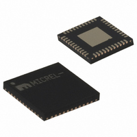
SY89540UMY Micrel Inc, SY89540UMY Datasheet - Page 5

SY89540UMY
Manufacturer Part Number
SY89540UMY
Description
IC XPOINT SW 4X4 PREC 44-MLF
Manufacturer
Micrel Inc
Series
SY89r
Datasheet
1.SY89540UMY.pdf
(14 pages)
Specifications of SY89540UMY
Function
Crosspoint Switch
Circuit
1 x 4:4
Voltage Supply Source
Single Supply
Voltage - Supply, Single/dual (±)
2.375 V ~ 2.625 V
Current - Supply
200mA
Operating Temperature
-40°C ~ 85°C
Mounting Type
Surface Mount
Package / Case
44-MLF®, QFN
Number Of Arrays
1
Differential Data Transmission
Yes
Power Supply Requirement
Single
Mounting
Surface Mount
Operating Temperature (max)
85C
Operating Temperature (min)
-40C
Operating Temperature Classification
Industrial
Cascading Capability
No
Line Code
NRZ
On-chip Buffers
No
On-chip Decoder
No
On-chip Latch Circuit
No
On-chip Mux/demux
No
Programmable
No
Dual Supply Voltage (typ)
Not RequiredV
Dual Supply Voltage (max)
Not RequiredV
Dual Supply Voltage (min)
Not RequiredV
Input Level
CML/LVDS/LVPECL
Output Level
LVDS
Lead Free Status / RoHS Status
Lead free / RoHS Compliant
Other names
576-3241
Available stocks
Company
Part Number
Manufacturer
Quantity
Price
Company:
Part Number:
SY89540UMY
Manufacturer:
VISHAY
Quantity:
2 568
Part Number:
SY89540UMY-TR
Manufacturer:
MICROCHIP/微芯
Quantity:
20 000
Functional Description
Buffer Mode
SY89540 can be used as a 1:4 fanout buffer. This is
the default mode with LOAD and CONFIG being HIGH
when the device is first powered up. The SIN0 and
SIN1 inputs select the input signal that will be buffered.
Regardless of the output switch selection, the input
signal will be buffered to all four outputs.
Crosspoint Mode
SY89540 can be programmed to take differential input
signals from any input and buffer the signals to one or
more outputs. Prior to configuring SIN and SOUT,
LOAD and CONFIG must be LOW. To program the
desired
sequence:
December 2007
1) Select the desired input with the SIN0 and
2) Pulse the LOAD with a positive pulse to load
3) Pulse the CONFIG pin with a positive pulse to
4) This
SIN1 inputs and the output with the SOUT0
and SOUT1.
SIN and SOUT.
latched the I/O configuration.
independent
outputs. Below is the truth table to create a 4:4
buffer where IN0 -> Q3, IN1 -> Q2, IN2 -> Q1,
and IN3 -> Q0:
Input
I/O
IN0
IN1
IN2
IN3
method
combination,
SIN1
paths
0
0
1
1
can
between
be
follow
SIN0
used
0
1
0
1
the
Table 1. 4:4 Buffer Truth Table
inputs
to
following
SOUT1
create
1
1
0
0
and
5
The SY89540 can be switched from crosspoint mode
to a 1:4 fanout buffer simply by providing a LOW-to-
HIGH pulse to the LOAD and CONFIG pins. The input
configuration (SIN0:1) will select the desired input
signal while the output switch will buffer the selected
input signal. To get the same desired input to all four
outputs (1:4), LOAD and CONFIG must be repeated
four times to cover all outputs (i.e., SOUT0:1 must go
through all four output combinations, repeated by
LOAD and CONFIG).
SOUT0
1
0
1
0
Load
0
0
0
0
hbwhelp@micrel.com
Config.
0
0
0
0
or (408) 955-1690
M9999-120607-C
Output
Q3
Q2
Q1
Q0


