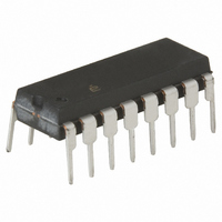
DG409DJZ Intersil, DG409DJZ Datasheet - Page 3

DG409DJZ
Manufacturer Part Number
DG409DJZ
Description
IC MULTIPLEXER DUAL 4X1 16DIP
Manufacturer
Intersil
Type
Analog Multiplexerr
Datasheet
1.DG408DJZ.pdf
(17 pages)
Specifications of DG409DJZ
Function
Multiplexer
Circuit
2 x 4:1
On-state Resistance
100 Ohm
Voltage Supply Source
Single, Dual Supply
Voltage - Supply, Single/dual (±)
5 V ~ 34 V, ±5 V ~ 20 V
Operating Temperature
-40°C ~ 85°C
Mounting Type
Through Hole
Package / Case
16-DIP (0.300", 7.62mm)
Package
16PDIP
Maximum On Resistance
100@±15V Ohm
Maximum Propagation Delay Bus To Bus
250@±15V@-40C to 85C|180(Typ)@12V ns
Maximum High Level Output Current
30 mA
Multiplexer Architecture
4:1
Maximum Turn-off Time
120(Typ)@12V ns
Maximum Turn-on Time
180(Typ)@12V ns
Power Supply Type
Single|Dual
Lead Free Status / RoHS Status
Lead free / RoHS Compliant
Available stocks
Company
Part Number
Manufacturer
Quantity
Price
Pin Descriptions - (DG408)
PIN
10
12
13
14
15
16
11
1
2
3
4
5
6
7
8
9
SYMBOL
GND
EN
V+
A
S
S
S
S
S
S
S
S
A
A
V-
D
0
1
2
3
4
8
7
6
5
2
1
Logic Decode Input (Bit 0, LSB)
Enable Input
Negative Power Supply Terminal
Source (Input) for Channel 1
Source (Input) for Channel 2
Source (Input) for Channel 3
Source (Input) for Channel 4
Drain (Output)
Source (Input) for Channel 8
Source (Input) for Channel 7
Source (Input) for Channel 6
Source (Input) for Channel 5
Positive Power Supply Terminal (Substrate)
Ground Terminal (Logic Common)
Logic Decode Input (Bit 2, MSB)
Logic Decode Input (Bit 1)
3
DESCRIPTION
DG408, DG409
Pin Descriptions - (DG409)
PIN
10
12
13
14
15
16
11
1
2
3
4
5
6
7
8
9
SYMBOL
GND
S
S
S
S
S
S
S
S
EN
D
D
V+
A
A
V-
1A
2A
3A
4A
4B
3B
2B
1B
A
B
0
1
Logic Decode Input (Bit 0, LSB)
Enable Input
Negative Power Supply Terminal
Source (Input) for Channel 1a
Source (Input) for Channel 2a
Source (Input) for Channel 3a
Source (Input) for Channel 4a
Drain a (Output a)
Drain b (Output b)
Source (Input) for Channel 4b
Source (Input) for Channel 3b
Source (Input) for Channel 2b
Source (Input) for Channel 1b
Positive Power Supply Terminal
Ground Terminal (Logic Common)
Logic Decode Input (Bit 1, MSB)
DESCRIPTION
June 13, 2006
FN3283.8


