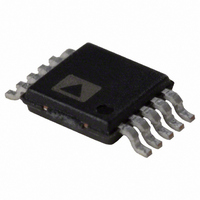
ADG1421BRMZ Analog Devices Inc, ADG1421BRMZ Datasheet - Page 8

ADG1421BRMZ
Manufacturer Part Number
ADG1421BRMZ
Description
IC SW SPST 2.1OHM RON 10MSOP
Manufacturer
Analog Devices Inc
Series
iCMOS®r
Datasheet
1.ADG1423BRMZ.pdf
(16 pages)
Specifications of ADG1421BRMZ
Function
Switch
Circuit
2 x SPST - NO
On-state Resistance
6.2 Ohm
Voltage Supply Source
Dual, Single, Dual Supply
Voltage - Supply, Single/dual (±)
±5V, 12V, ±15V
Current - Supply
120µA
Operating Temperature
-40°C ~ 125°C
Mounting Type
Surface Mount
Package / Case
10-TFSOP, 10-MSOP (0.118", 3.00mm Width)
Analog Switch Type
SPST
No. Of Channels
2
Bandwidth
180MHz
On State Resistance Max
2.1ohm
Turn Off Time
115ns
Turn On Time
115ns
Supply Voltage Range
13.5V To 16.5V
Lead Free Status / RoHS Status
Lead free / RoHS Compliant
Available stocks
Company
Part Number
Manufacturer
Quantity
Price
Company:
Part Number:
ADG1421BRMZ
Manufacturer:
Analog Devices Inc
Quantity:
135
Part Number:
ADG1421BRMZ
Manufacturer:
ADI/亚德诺
Quantity:
20 000
Part Number:
ADG1421BRMZ-REEL7
Manufacturer:
ADI/亚德诺
Quantity:
20 000
ADG1421/ADG1422/ADG1423
PIN CONFIGURATION AND FUNCTION DESCRIPTIONS
Table 7. 10-Lead LFCSP Pin Function Descriptions
Pin No.
1
2
3
4
5
6
7
8
9
10
Table 9. ADG1421/ADG1422 Truth Table
ADG1421 INx
1
0
Table 10. ADG1423 Truth Table
ADG1423 INx
0
1
Mnemonic
S1
S2
NC
GND
V
IN2
IN1
V
D2
D1
EPAD
DD
SS
NOTES
1. EXPOSED PAD TIED TO SUBSTRATE, V
2. NC = NO CONNECT
Figure 4. 10-Lead LFCSP Pin Configuration
GND
V
NC
S1
S2
DD
1
2
3
4
5
(Not to Scale)
ADG1421/
ADG1422/
Description
Source Terminal. This pin can be an
input or output.
Source Terminal. This pin can be an
input or output.
No Connect.
Ground (0 V) Reference.
Most Positive Power Supply Potential.
Logic Control Input.
Logic Control Input.
Most Negative Power Supply Potential.
Drain Terminal. This pin can be an
input or output.
Drain Terminal. This pin can be an
input or output.
Exposed pad tied to substrate, V
ADG1423
TOP VIEW
10 D1
9
8
7
6
D2
V
IN1
IN2
SS
ADG1422 INx
0
1
Switch 1 Condition
Off
On
SS
.
SS
.
Rev. 0 | Page 8 of 16
Table 8. 10-Lead MSOP Pin Function Descriptions
Pin No.
1
2
3
4
5
6
7
8
9
10
Mnemonic
S1
S2
NC
GND
V
IN2
IN1
V
D2
D1
DD
SS
On
Off
Switch Condition
Switch 2 Condition
On
Off
Figure 5. 10-Lead MSOP Pin Configuration
GND
V
NC
S1
S2
DD
1
2
3
4
5
NC = NO CONNECT
Description
Source Terminal. This pin can be an
input or output.
Source Terminal. This pin can be an
input or output.
No Connect.
Ground (0 V) Reference.
Most Positive Power Supply Potential.
Logic Control Input.
Logic Control Input.
Most Negative Power Supply Potential.
Drain Terminal. This pin can be an
input or output.
Drain Terminal. This pin can be an
input or output.
ADG1421/
ADG1422/
(Not to Scale)
ADG1423
TOP VIEW
10
9
8
7
6
D1
D2
V
IN1
IN2
SS


