ADG509ATQ Analog Devices Inc, ADG509ATQ Datasheet - Page 2
ADG509ATQ
Manufacturer Part Number
ADG509ATQ
Description
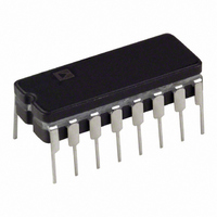
IC MULTIPLEXER DUAL 4X1 16CDIP
Manufacturer
Analog Devices Inc
Type
Analog Multiplexerr
Datasheet
1.ADG509AKRZ-REEL7.pdf
(16 pages)
Specifications of ADG509ATQ
Rohs Status
RoHS non-compliant
Function
Multiplexer
Circuit
2 x 4:1
On-state Resistance
300 Ohm
Voltage Supply Source
Dual Supply
Voltage - Supply, Single/dual (±)
±10.8 V ~ 16.5 V
Current - Supply
20µA
Operating Temperature
-55°C ~ 125°C
Mounting Type
Through Hole
Package / Case
16-CDIP (0.300", 7.62mm)
Msl
MSL 1 - Unlimited
Peak Reflow Compatible (260 C)
No
Leaded Process Compatible
No
Package
16CDIP
Maximum On Resistance
700@16.5V Ohm
Maximum Propagation Delay Bus To Bus
300@±16.5V|450@16.5V ns
Maximum High Level Output Current
20 mA
Multiplexer Architecture
4:1
Number Of Channels Per Chip
1
Maximum Turn-on Time
450@16.5V ns
Power Supply Type
Single|Dual
Lead Free Status / RoHS Status
Contains lead / RoHS non-compliant
Available stocks
Company
Part Number
Manufacturer
Quantity
Price


ADG508A/ADG509A
TABLE OF CONTENTS
Features .............................................................................................. 1
Functional Block Diagrams ............................................................. 1
General Description ......................................................................... 1
Product Highlights ........................................................................... 1
Revision History ............................................................................... 2
Specifications ..................................................................................... 3
REVISION HISTORY
7/09—Rev. C to Rev. D
Changes to Table 4 ............................................................................ 8
3/07—Rev. B to Rev. C
Updated Format .................................................................. Universal
Changes to Table 3 ............................................................................ 6
Inserted Table 4 ................................................................................. 7
Inserted Table 6 ................................................................................. 8
Changes to Figure 24 ...................................................................... 12
Updated Outline Dimensions ....................................................... 13
Changes to Ordering Guide .......................................................... 15
Dual Supply ................................................................................... 3
Single Supply ................................................................................. 5
Rev. D | Page 2 of 16
Absolute Maximum Ratings ............................................................7
Pin Configurations and Function Descriptions ............................8
Typical Performance Characteristics ........................................... 10
Test Circuits ..................................................................................... 11
Single-Supply Octal DAC Application ........................................ 13
Outline Dimensions ....................................................................... 14
ESD Caution...................................................................................7
Ordering Guide .......................................................................... 16
Related parts for ADG509ATQ
Image
Part Number
Description
Manufacturer
Datasheet
Request
R

Part Number:
Description:
±1.7g Dual-Axis IMEMS Accelerometer Evaluation Board
Manufacturer:
Analog Devices Inc
Datasheet:

Part Number:
Description:
Inertial Sensor Evaluation System
Manufacturer:
Analog Devices Inc
Datasheet:
Part Number:
Description:
Manufacturer:
Analog Devices Inc
Datasheet:
Part Number:
Description:
Manufacturer:
Analog Devices Inc
Datasheet:
Part Number:
Description:
Manufacturer:
Analog Devices Inc
Datasheet:
Part Number:
Description:
Manufacturer:
Analog Devices Inc
Datasheet:
Part Number:
Description:
Manufacturer:
Analog Devices Inc
Datasheet:
Part Number:
Description:
Manufacturer:
Analog Devices Inc
Datasheet:
Part Number:
Description:
Manufacturer:
Analog Devices Inc
Datasheet:
Part Number:
Description:
Manufacturer:
Analog Devices Inc
Datasheet:
Part Number:
Description:
Manufacturer:
Analog Devices Inc
Datasheet:
Part Number:
Description:
Manufacturer:
Analog Devices Inc
Datasheet:
Part Number:
Description:
Manufacturer:
Analog Devices Inc
Datasheet: