ISL54405IRTZ-T Intersil, ISL54405IRTZ-T Datasheet
ISL54405IRTZ-T
Specifications of ISL54405IRTZ-T
Available stocks


Related parts for ISL54405IRTZ-T

ISL54405IRTZ-T Summary of contents
Page 1
... All other trademarks mentioned are the property of their respective owners. ISL54405 June 5, 2008 FN6699.1 Signal Switching from 3. Supply RMS 5V_Supply VDD ISL54405 LOGIC AND CLICK/POP CONTROL L GND | Intersil (and design registered trademark of Intersil Americas Inc. Copyright Intersil Americas Inc. 2008. All Rights Reserved TQFN µ CAP_SS ...
Page 2
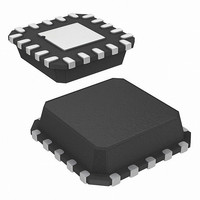
Pinouts (Note 1) ISL54405 (16 LD µTQFN) TOP VIEW MUTE SEL NOTE: 1. See Page 1 for ISL54405 Block Diagram. 2 ISL54405 MUTE ...
Page 3
... ISL54405IVZ 54405 IVZ (Note 2) ISL54405IVZ-T* 54405 IVZ (Note 2) ISL54405IRTZ (Note 2) 05TZ ISL54405IRTZ-T* 05TZ (Note 2) ISL54405IRUZ-T* GAD (Note 3) *Please refer to TB347 for details on reel specifications. NOTES: 2. These Intersil Pb-free plastic packaged products employ special Pb-free material sets; molding compounds/die attach materials and 100% matte tin plate PLUS ANNEAL - e3 termination finish, which is RoHS compliant and compatible with both SnPb and Pb-free soldering operations ...
Page 4
... Ld µTQFN Package (Note 0.3V Maximum Junction Temperature (Plastic Package +150°C DD Maximum Storage Temperature Range . . . . . . . . . . . -65°C to +150° 0.3V) Pb-free reflow profile . . . . . . . . . . . . . . . . . . . . . . . . . .see link below DD http://www.intersil.com/pbfree/Pb-FreeReflow.asp Operating Conditions Temperature Range . . . . . . . . . . . . . . . . . . . . . . . . . -40°C to +85°C Test Conditions +3.0V to +3.6V, GND = 0V Float ...
Page 5
Electrical Specifications - 3.3V Supply PARAMETER Insertion Loss 1kHz LOAD Gain vs Frequency 20Hz to 20kHz 1kHz ON Stereo Channel Imbalance f = 20Hz to 20kHz ...
Page 6
Electrical Specifications - 3.3V Supply PARAMETER Positive Supply Current +3.6V +3.6V +3.6V DIGITAL INPUT CHARACTERISTICS Input Voltage Low SELL V MUTEL Input Voltage High, V ...
Page 7
Test Circuits and Waveforms V DD LOGIC INPUT 0V SWITCH OUTPUT V OUT 0V FIGURE 2A. MEASUREMENT POINTS SIGNAL MUTE GENERATOR ANALYZER GND R L Signal direction through switch is reversed, worst case values are ...
Page 8
Sound Card AC Coupled Application Block Diagrams LOGIC µCONTROLLER L AUDIO CODEC R LOGIC µCONTROLLER L FRONT PANEL LINE OUT OR HEAD-PHONE JACK R Detailed Description The ISL54405 is a single supply, bi-directional, dual single pole/double throw (SPDT) ultra low ...
Page 9
SPDT Switch Cell Architecture and Performance Characteristics The normally open ( and normally closed ( the SPDT switches are T-Type switches that have a typical r of 1.9Ω and an off-isolation of >120dB. The low ...
Page 10
MUTE TO ON When the Mute pin is driven LOW the ISL54405 will transition to the ON-state in the following sequence: 1. All active shunt switches turn-off quickly. 2. The resistance of the switches selected by the SEL pin will ...
Page 11
COM side (L,R) are activated and inoperable on the signal side (L1, R1, L2, R2) of the switch. When DIR_SEL = Logic “0” the C/P shunts are activated on the signal side (L1, R1, L2, R2) and inoperable on the ...
Page 12
V must be applied before any input signals, and DD the signal voltages must remain between V the logic voltage must remain between V If these conditions cannot be guaranteed, then precautions must be implemented to prohibit the current ...
Page 13
Typical Performance Curves 3 3.3V DD +85° 80mA COM 2.5 2.0 +25°C 1.5 -40°C 1.0 0 (V) COM FIGURE 9. ON-RESISTANCE vs SWITCH VOLTAGE 3.3V OR V_Supply ...
Page 14
Typical Performance Curves 0.05 0.04 0.03 0.02 0.01 0.00 -0.01 -0.02 -0.03 -0.04 -0.05 20 100 1k FREQUENCY (Hz) FIGURE 15. GAIN vs FREQUENCY - 3. 32Ω LOAD -94 A-WEIGHTED FILTER -96 -98 -100 ...
Page 15
Typical Performance Curves -100 V = 3.3V -101 DD -102 R = 20kΩ LOAD -103 10Hz to 30k FILTER -104 -105 -106 1.7V -107 RMS -108 -109 -110 -111 1.6V RMS -112 -113 -114 1.5V -115 -116 -117 -118 -119 ...
Page 16
Typical Performance Curves 80 LEFT INPUT 60 40 4.6V/s LEFT OUTPUT 20 0 RIGHT OUTPUT -20 4.6V/s -40 RIGHT INPUT - 3.3V DD CAP_SS = 0.1µF -80 -100 -80 -60 -40 - TIME (ms) FIGURE 27. ...
Page 17
Thin Shrink Small Outline Plastic Packages (TSSOP) N INDEX 0.25(0.010) E AREA E1 - 0.05(0.002) SEATING PLANE - -C- α 0.10(0.004) 0.10(0.004 NOTES: 1. These package ...
Page 18
... L 7. Maximum package warpage is 0.05mm. 8. Maximum allowable burrs is 0.076mm in all directions. 9. JEDEC Reference MO-255. TERMINAL TIP 10. For additional information, to assist with the PCB Land Pattern Design effort, see Intersil Technical Brief TB389. 1.40 0.40 0.20 MILLIMETERS MIN NOMINAL ...
Page 19
... Accordingly, the reader is cautioned to verify that data sheets are current before placing orders. Information furnished by Intersil is believed to be accurate and reliable. However, no responsibility is assumed by Intersil or its subsidiaries for its use; nor for any infringements of patents or other rights of third parties which may result from its use ...