ISL54057IRUZ-T Intersil, ISL54057IRUZ-T Datasheet
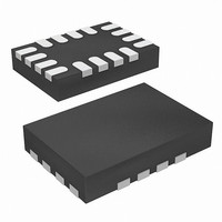
IC SWITCH 4X1 16UTQFN

ISL54057IRUZ-T

Manufacturer Part Number
ISL54057IRUZ-T
Description
IC SWITCH 4X1 16UTQFN
Manufacturer
Intersil
Datasheet

Specifications of ISL54057IRUZ-T

Function
Switch
Circuit
1 x 4:1
On-state Resistance
750 mOhm
Voltage Supply Source
Single Supply
Voltage - Supply, Single/dual (±)
1.6 V ~ 3.6 V
Current - Supply
.05µA
Operating Temperature
-40°C ~ 85°C
Mounting Type
Surface Mount
Package / Case
16-UTQFN (16-µTQFN)
Lead Free Status / RoHS Status
Lead free / RoHS Compliant
Ultra Low ON-Resistance, Low-Voltage,
Single Supply, Differential 4 to 1 Analog
Multiplexer
The Intersil ISL54057 device contains precision, bidirectional,
analog switches configured as a differential 4-channel
multiplexer/demultiplexer, designed to operate from a single
+1.6V to +3.6V supply. The devices have an inhibit pin to
simultaneously open all signal paths.
ON resistance is 0.41Ω with a +3V supply and 0.61Ω with a
single +1.8V supply. Each switch can handle rail to rail
analog signals. The off-leakage current is only 4nA max at
+25°C or 35nA max at +85°C with a +3.3V supply.
All digital inputs are 1.8V logic-compatible when using a
single +3V supply.
The ISL54057 is a differential 4 to 1 multiplexer device that is
offered in a 16 Ld 2.6x1.8x0.5mm µTQFN package.
Table 1 summarizes the performance of this family.
Related Literature
• Technical Brief TB363 “Guidelines for Handling and
• Application Note AN557 “Recommended Test Procedures
Ordering Information
NOTE: Intersil Pb-free products employ special Pb-free material sets; molding compounds/die attach materials and 100% matte tin plate termination
finish, which are RoHS compliant and compatible with both SnPb and Pb-free soldering operations. Intersil Pb-free products are MSL classified at Pb-
free peak reflow temperatures that meet or exceed the
Pb-free requirements of IPC/JEDEC J STD-020C.
ISL54057IRUZ-T
Configuration
3V R
3V t
1.8V R
1.8V t
Packages
PART NUMBER (NOTE)
Processing Moisture Sensitive Surface Mount Devices
(SMDs)”
for Analog Switches”
ON
ON
ON
ON
/t
OFF
/t
OFF
TABLE 1. FEATURES AT A GLANCE
GAB
®
PART MARKING
1
Diff 4:1 Mux
0.41Ω
27ns/18ns
0.61Ω
34ns/26ns
16 Ld 2.6x1.8x0.5mm µTQFN
Data Sheet
ISL54057
TEMP. RANGE (°C)
-40 to +85
1-888-INTERSIL or 1-888-468-3774
CAUTION: These devices are sensitive to electrostatic discharge; follow proper IC Handling Procedures.
Features
• Pb-Free Plus Anneal Available (RoHS Compliant)
• ON Resistance (R
• R
• R
• Single Supply Operation. . . . . . . . . . . . . . . . . +1.6V to +3.6V
• Low Power Consumption (PD). . . . . . . . . . . . . . . . . <0.18µW
• Fast Switching Action (V
• Break-Before-Make
• High Current Handling Capacity (300mA Continuous)
• Available in 16 Ld 2.6x1.8x0.5mm µTQFN
• 1.8V CMOS-Logic Compatible (+3V Supply)
Applications
• Battery Powered, Handheld, and Portable Equipment
• Portable Test and Measurement
• Medical Equipment
• Audio and Video Switching
16 Ld Thin µQFN Tape and Reel (Pb-free) L16.2.6x1.8A
September 29, 2006
- V+ = +3.0V . . . . . . . . . . . . . . . . . . . . . . . . . . . . . 0.41Ω
- V+ = +1.8V . . . . . . . . . . . . . . . . . . . . . . . . . . . . . 0.61Ω
- t
- t
- Cellular/Mobile Phones
- Pagers
- Laptops, Notebooks, Palmtops
ON
ON
ON
OFF
Matching Between Channels. . . . . . . . . . . . . . . . 0.09Ω
Flatness Across Signal Range . . . . . . . . . . . . . . 0.07Ω
All other trademarks mentioned are the property of their respective owners.
. . . . . . . . . . . . . . . . . . . . . . . . . . . . . . . . . . . . 27ns
. . . . . . . . . . . . . . . . . . . . . . . . . . . . . . . . . . . 18ns
|
Intersil (and design) is a registered trademark of Intersil Americas Inc.
PACKAGE
Copyright Intersil Americas Inc. 2006. All Rights Reserved
ON
)
S
= +3V)
ISL54057
PKG. DWG. #
FN6379.0

Related parts for ISL54057IRUZ-T

ISL54057IRUZ-T Summary of contents

Page 1

... Ordering Information PART NUMBER (NOTE) PART MARKING ISL54057IRUZ-T GAB NOTE: Intersil Pb-free products employ special Pb-free material sets; molding compounds/die attach materials and 100% matte tin plate termination finish, which are RoHS compliant and compatible with both SnPb and Pb-free soldering operations. Intersil Pb-free products are MSL classified at Pb- free peak reflow temperatures that meet or exceed the Pb-free requirements of IPC/JEDEC J STD-020C ...

Page 2

Pinouts (Note 1) NOTE: 1. 2.6mm x 1.8mm x 0.5mm Truth Table ISL54057 INH ADD0 ADD1 NOTE: Logic “0” ≤0.5V. Logic “1” ≥1.4V, with a ...

Page 3

... Maximum Junction Temperature (Plastic Package +150°C Maximum Storage Temperature Range -65°C to +150°C Maximum Lead Temperature (Soldering 10s +300°C (Lead Tips Only) Operating Conditions Temperature Range ISL54057IRUZ . . . . . . . . . . . . . . . . . . . . . . . . . . . . . -40°C to +85°C Test Conditions +2.7V to +3.3V, GND = 0V, V SUPPLY (Notes 4, 8), Unless Otherwise Specified TEST CONDITIONS ...

Page 4

Electrical Specifications: 3V Supply PARAMETER OFF Isolation R = 50Ω (See Figures 3 and 5) Crosstalk, Note 9 POWER SUPPLY CHARACTERISTICS Power Supply Range Positive Supply Current 3.3V, V NOTES Input voltage ...

Page 5

Test Circuits and Waveforms V+ LOGIC 50% INPUT VA0, VB0 90% SWITCH OUTPUT 0V t OFF Logic input waveform is inverted for switches that have the opposite logic sense. FIGURE 1A. INHIBIT t /t MEASUREMENT POINTS ...

Page 6

Test Circuits and Waveforms V+ LOGIC INPUT 0V SWITCH OUTPUT V OUT 0V t BBM FIGURE 2A. t MEASUREMENT POINTS BBM V+ 10nF SIGNAL GENERATOR ANALYZER COMx GND R L Off-Isolation is measured between COM and “Off” ...

Page 7

Test Circuits and Waveforms V+ C SIGNAL GENERATOR ADD1 ADD0 Channel Select ANALYZER COM B GND R L Crosstalk is measured between adjacent channels with one channel ON and the other channel OFF. Signal direction ...

Page 8

Power-Supply Considerations The ISL54057 construction is typical of most CMOS analog switches, in that they have two supply pins: V+ and GND. V+ and GND drive the internal CMOS switches and set their analog voltage limits. Unlike switches with a ...

Page 9

... Accordingly, the reader is cautioned to verify that data sheets are current before placing orders. Information furnished by Intersil is believed to be accurate and reliable. However, no responsibility is assumed by Intersil or its subsidiaries for its use; nor for any infringements of patents or other rights of third parties which may result from its use ...

Page 10

... L 7. Maximum package warpage is 0.05mm. 8. Maximum allowable burrs is 0.076mm in all directions. 9. JEDEC Reference MO-255. TERMINAL TIP 10. For additional information, to assist with the PCB Land Pattern Design effort, see Intersil Technical Brief TB389. 1.40 0.40 0.20 MILLIMETERS MIN NOMINAL ...

Related keywords