HI1-0539-5 Intersil, HI1-0539-5 Datasheet - Page 2
HI1-0539-5
Manufacturer Part Number
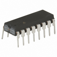
HI1-0539-5
Description
IC MULTIPLEXER 4X1 16CDIP
Manufacturer
Intersil
Datasheet
1.HI1-0539-5.pdf
(12 pages)
Specifications of HI1-0539-5
Function
Multiplexer
Circuit
1 x 4:1
On-state Resistance
850 Ohm
Voltage Supply Source
Dual Supply
Voltage - Supply, Single/dual (±)
±5 V ~ 18 V
Current - Supply
0.001mA
Operating Temperature
0°C ~ 75°C
Mounting Type
Through Hole
Package / Case
16-CDIP (0.300", 7.62mm)
Lead Free Status / RoHS Status
Contains lead / RoHS non-compliant
Available stocks
Company
Part Number
Manufacturer
Quantity
Price


Absolute Maximum Ratings
V+ to V- . . . . . . . . . . . . . . . . . . . . . . . . . . . . . . . . . . . . . . . . . . . 40V
V+ or V- to GND. . . . . . . . . . . . . . . . . . . . . . . . . . . . . . . . . . . . . 20V
Analog Signal (V
Digital Input Voltage (V
Analog Current (IN or OUT) . . . . . . . . . . . . . . . . . . . . . . . . . . . 20mA
Operating Conditions
Temperature Range
CAUTION: Stresses above those listed in “Absolute Maximum Ratings” may cause permanent damage to the device. This is a stress only rating and operation of the
device at these or any other conditions above those indicated in the operational sections of this specification is not implied.
NOTE:
Electrical Specifications
DYNAMIC CHARACTERISTICS
Access Time, t
Break-Before-Make Delay, t
Enable Delay (ON), t
Enable Delay (OFF), t
Settling Time
Charge Injection (Output)
∆ Charge Injection (Output)
Charge Injection (Input)
Differential Crosstalk
Single Ended Crosstalk
Channel Input Capacitance, C
Channel Output Capacitance, C
Channel On Output Capacitance, C
Input to Output Capacitance, C
Digital Input Capacitance, C
DIGITAL INPUT CHARACTERISTICS
Input Low Threshold, V
Input High Threshold, V
Input Leakage Current (High), I
Input Leakage Current (Low), I
ANALOG CHANNEL CHARACTERISTICS
Analog Signal Range, V
1. θ
HI-539-5 . . . . . . . . . . . . . . . . . . . . . . . . . . . . . . . . . . 0
JA
is measured with the component mounted on an evaluation PC board in free air.
A
IN
, V
OUT
ON(EN)
OFF(EN)
EN
AL
AH
IN
) . . . . . . . . . . . . . . . . . . . . . . . . . V- to V+
, V
PARAMETER
A
OPEN
A
) . . . . . . . . . . . . . . . . . . . . . . V- to V+
S(OFF)
AL
DS(OFF)
AH
D(OFF)
2
Supplies =
Unless Otherwise Specified
D(ON)
±
15V, V
EN
o
C to 75
= 4V, V
o
C
AH
HI-539
(Logic Level High) = 4V, V
To 0.01%
Note 4
Note 4
Note 5
CONDITIONS
Thermal Information
Thermal Resistance (Typical, Note 1)
Maximum Junction Temperature
Maximum Storage Temperature Range . . . . . . . . . -65
Maximum Lead Temperature (Soldering 10s) . . . . . . . . . . . . .300
TEST
CERDIP Package. . . . . . . . . . . . . . . . .
Ceramic Package. . . . . . . . . . . . . . . . . . . . . . . . . . . . . . . . 175
Plastic Package . . . . . . . . . . . . . . . . . . . . . . . . . . . . . . . . . 150
TEMP
(
Full
Full
Full
Full
Full
Full
Full
Full
Full
Full
Full
Full
Full
Full
Full
Full
Full
o
25
25
25
25
25
25
25
C)
AL
(Logic Level Low) = 0.8V,
MIN
-10
4.0
30
30
-
-
-
-
-
-
-
-
-
-
-
-
-
-
-
-
-
-
-
-
TYP
-124
-100
0.08
250
250
160
0.9
0.1
85
10
17
3
5
7
3
-
-
-
-
-
-
-
-
-
θ
JA
(
75
o
1,000
1,000
MAX
C/W) θ
750
750
650
900
+10
0.8
1
1
-
-
-
-
-
-
-
-
-
-
-
-
-
-
o
C to 150
JC
UNITS
(
20
pC
pC
pC
dB
dB
µA
µA
µs
pF
pF
pF
pF
pF
ns
ns
ns
ns
ns
ns
ns
ns
o
V
V
V
C/W)
o
o
o
o
C
C
C
C
Related parts for HI1-0539-5
Image
Part Number
Description
Manufacturer
Datasheet
Request
R

Part Number:
Description:
HI1-303-5IC,ANALOG SWITCH,DUAL,SPDT,CMOS,DIP,14PIN
Manufacturer:
Intersil Corporation
Datasheet:
Part Number:
Description:
300 MIL PDIP/CDIP//MUX DIFF 4:1 OVP 16CDIP /883
Manufacturer:
Intersil Corporation
Part Number:
Description:
DAC 12BIT 6.7MHZ 0.25LSB 24 S/B DIP /883
Manufacturer:
Intersil Corporation
Datasheet:

Part Number:
Description:
IC ADC 12BIT 40KSPS 1CH 28-SBDIP
Manufacturer:
Intersil
Datasheet:
Part Number:
Description:
IC ADC 12BIT 40KSPS 1CH 28-SBDIP
Manufacturer:
Intersil
Datasheet:
Part Number:
Description:
IC ADC 12BIT 67KSPS 1CH 28-SBDIP
Manufacturer:
Intersil
Datasheet:
Part Number:
Description:
IC ADC 12BIT 40KSPS 1CH 28-SBDIP
Manufacturer:
Intersil
Datasheet:
Part Number:
Description:
IC ADC 12BIT 40KSPS 1CH 28-SBDIP
Manufacturer:
Intersil
Datasheet:

Part Number:
Description:
CONV D/A 12BIT 6.7MHZ 24-DIP
Manufacturer:
Intersil
Datasheet:
Part Number:
Description:
CONV D/A 12BIT 6.7MHZ 24-DIP
Manufacturer:
Intersil
Datasheet:

Part Number:
Description:
IC SWITCH QUAD SPST 16CDIP
Manufacturer:
Intersil
Datasheet:
Part Number:
Description:
IC MULTIPLEXER 8X1 16CDIP
Manufacturer:
Intersil
Datasheet:
Part Number:
Description:
IC SWITCH QUAD SPST 16CDIP
Manufacturer:
Intersil
Datasheet: