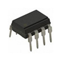
AD743JN Analog Devices Inc, AD743JN Datasheet - Page 8

AD743JN
Manufacturer Part Number
AD743JN
Description
Manufacturer
Analog Devices Inc
Type
General Purpose Amplifierr
Datasheet
1.AD743JN.pdf
(12 pages)
Specifications of AD743JN
Rail/rail I/o Type
No
Number Of Elements
1
Unity Gain Bandwidth Product
4.5MHz
Slew Rate
2.8V/us
Common Mode Rejection Ratio
80dB
Input Offset Voltage
1mV
Input Bias Current
200pA
Single Supply Voltage (typ)
Not RequiredV
Dual Supply Voltage (typ)
±15V
Voltage Gain In Db
132.04dB
Power Supply Rejection Ratio
90dB
Power Supply Requirement
Dual
Shut Down Feature
No
Single Supply Voltage (min)
Not RequiredV
Single Supply Voltage (max)
Not RequiredV
Dual Supply Voltage (min)
±4.8V
Dual Supply Voltage (max)
±18V
Technology
BiFET
Operating Temp Range
0C to 70C
Operating Temperature Classification
Commercial
Mounting
Through Hole
Pin Count
8
Package Type
PDIP
Lead Free Status / Rohs Status
Not Compliant
Available stocks
Company
Part Number
Manufacturer
Quantity
Price
AD743
Figures 4 and 5 show two ways to buffer and amplify the output of
a charge output transducer. Both require using an amplifier that
has a very high input impedance, such as the AD743. Figure 4
shows a model of a charge amplifier circuit. Here, amplifica-
tion depends on the principle of conservation of charge at the
input of amplifier A1, which requires that the charge on capaci-
tor C
voltage of ∆Q/C
the output amplified by the noise gain (1 + (C
The circuit in Figure 5 is simply a high impedance follower with
gain. Here the noise gain (1 + (R1/R2)) is the same as the gain
from the transducer to the output. In both circuits, resistor R
required as a dc bias current return.
There are three important sources of noise in these circuits.
Amplifiers A1 and A2 contribute both voltage and current noise,
while resistor R
where
k = Boltzman’s Constant = 1.381 × 10
T = Absolute Temperature, kelvin (0°C = 273.2 kelvin)
This must be root-sum-squared with the amplifier’s own
current noise.
Figure 6 shows that these circuits in Figures 4 and 5 have an
identical frequency response and noise performance (provided
that C
network is used to increase the effective resistance of R
improve the low frequency cutoff point by the same factor.
f = Bandwidth—in Hz (assuming an ideal “brick wall” filter)
S
Figure 5. Model for a High Z Follower with Gain
S
/C
be transferred to capacitor C
F
= R1/ R2). One feature of the first circuit is that a “T”
Figure 4. Charge Amplifier Circuit
F
B
. The amplifier’s input voltage noise will appear at
contributes a current noise of
R2
*OPTIONAL, SEE TEXT
C
S
*OPTIONAL, SEE TEXT
C
˜ N
B
*
= 4
C
R
C
R
B
B
S
B
R
*
*
*
B
A1
*
k
R
R
C
B
T
F
B
R2
A2
R1
R2
F
R1
R1
∆
, thus yielding an output
–23
f
=
C
C
joules/kelvin
S
F
S
/C
F
)) of the circuit.
B
and to
B
is
–8–
However, this does not change the noise contribution of R
in this example, dominates at low frequencies. The graph of
Figure 7 shows how to select an R
this resistor’s contribution to overall circuit noise. When the
equivalent current noise of R
(√2qIB), there is diminishing return in making R
To maximize dc performance over temperature, the source
resistances should be balanced on each input of the amplifier.
This is represented by the optional resistor R
As previously mentioned, for best noise performance, care should
be taken to also balance the source capacitance designated by C
The value for C
At values of C
noise; capacitor C
or greater.
Figure 6. Noise at the Outputs of the Circuits of
Figures 4 and 5. Gain = +10, C
Figure 7. Graph of Resistance vs. Input Bias Current
Where the Equivalent Noise √4kT/R , Equals the Noise
of the Bias Current √2qI
5.2
5.2
5.2
5.2
5.2
–100
–110
–120
–130
–140
–150
–160
–170
–180
–190
–200
–210
–220
10
10
10
10
10
10
0.01
9
8
7
6
1pA
B
B
over 300 pF, there is a diminishing impact on
0.1
in Figure 4 would be equal to C
B
can then be simply a large bypass of 0.01 µF
10pA
1
INPUT BIAS CURRENT
FREQUENCY (Hz)
B
B
((√4kT)/R equals the noise of I
10
R
DUE TO
B
100pA
B
NOISE
S
ALONE
large enough to minimize
= 3000 pF, R
100
I
B
DUE TO
NOISE
ALONE
B
1k
in Figures 4 and 5.
1nA
OUTPUT
TOTAL
B
NOISE
S
larger.
B
10k
in Figure 5.
= 22 M Ω
B
REV. E
100k
which,
10nA
B
B
.


