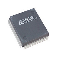
EPM7256AQC208-10 Altera, EPM7256AQC208-10 Datasheet - Page 17

EPM7256AQC208-10
Manufacturer Part Number
EPM7256AQC208-10
Description
Manufacturer
Altera
Datasheet
1.EPM7256AQC208-10.pdf
(64 pages)
Specifications of EPM7256AQC208-10
Family Name
MAX 7000A
Memory Type
EEPROM
# Macrocells
256
Number Of Usable Gates
5000
Frequency (max)
125MHz
Propagation Delay Time
10ns
Number Of Logic Blocks/elements
16
# I/os (max)
164
Operating Supply Voltage (typ)
3.3V
In System Programmable
Yes
Operating Supply Voltage (min)
3V
Operating Supply Voltage (max)
3.6V
Operating Temp Range
0C to 70C
Operating Temperature Classification
Commercial
Mounting
Surface Mount
Pin Count
208
Package Type
PQFP
Lead Free Status / Rohs Status
Not Compliant
Available stocks
Company
Part Number
Manufacturer
Quantity
Price
Company:
Part Number:
EPM7256AQC208-10
Manufacturer:
MAXIM
Quantity:
5 510
Altera Corporation
f
For more information on using the Jam STAPL language, see
Note 88 (Using the Jam Language for ISP & ICR via an Embedded Processor)
and
Processor).
ISP circuitry in MAX 7000AE devices is compliant with the IEEE Std. 1532
specification. The IEEE Std. 1532 is a standard developed to allow
concurrent ISP between multiple PLD vendors.
Programming Sequence
During in-system programming, instructions, addresses, and data are
shifted into the MAX 7000A device through the TDI input pin. Data is
shifted out through the TDO output pin and compared against the
expected data.
Programming a pattern into the device requires the following six ISP
stages. A stand-alone verification of a programmed pattern involves only
stages 1, 2, 5, and 6.
1.
2.
3.
4.
5.
6.
Application Note 122 (Using Jam STAPL for ISP & ICR via an Embedded
Enter ISP. The enter ISP stage ensures that the I/O pins transition
smoothly from user mode to ISP mode. The enter ISP stage requires
1 ms.
Check ID. Before any program or verify process, the silicon ID is
checked. The time required to read this silicon ID is relatively small
compared to the overall programming time.
Bulk Erase. Erasing the device in-system involves shifting in the
instructions to erase the device and applying one erase pulse of
100 ms.
Program. Programming the device in-system involves shifting in the
address and data and then applying the programming pulse to
program the EEPROM cells. This process is repeated for each
EEPROM address.
Verify. Verifying an Altera device in-system involves shifting in
addresses, applying the read pulse to verify the EEPROM cells, and
shifting out the data for comparison. This process is repeated for
each EEPROM address.
Exit ISP. An exit ISP stage ensures that the I/O pins transition
smoothly from ISP mode to user mode. The exit ISP stage requires
1 ms.
MAX 7000A Programmable Logic Device Data Sheet
Application
17


