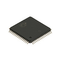
CY7C4245V-15ASC Cypress Semiconductor Corp, CY7C4245V-15ASC Datasheet

CY7C4245V-15ASC
Specifications of CY7C4245V-15ASC
Available stocks
Related parts for CY7C4245V-15ASC
CY7C4245V-15ASC Summary of contents
Page 1
... High-speed, low-power, first-in first-out (FIFO) memories • (CY7C4425V) • 256 x 18 (CY7C4205V) • 512 x 18 (CY7C4215V) • (CY7C4225V) • (CY7C4235V) • (CY7C4245V) • 0.65µ CMOS • High-speed 67-MHz operation (15-ns read/write cycle times) • Low power — • ...
Page 2
... WRITE POINTER RESET LOGIC THREE–STATE OUTPUT REGISTER EXPANSION LOGIC Q 0–17 STQFP/TQFP Top View CY7C4425V 6 10 CY7C4205V CY7C4215V CY7C4225V CY7C4235V CY7C4245V CY7C4225V/4205V/4215V CY7C4425V/4235V/4245V FLAG PROGRAM REGISTER FF EF FLAG PAE LOGIC PAF SMODE READ POINTER READ CONTROL OE RCLK REN GND ...
Page 3
... CY7C4225V CY7C4235V 64-pin 14x14 64-pin 14x14 TQFP TQFP 64-pin 10x10 64-pin 10x10 STQFP STQFP Function /SMODE is tied CC /SMODE is tied are written (read) into (from) the program standard mode of width CC Unit MHz CY7C4245V 64-pin 14x14 TQFP 64-pin 10x10 STQFP /SMODE Retransmit Page ...
Page 4
Pin Definitions (continued) Signal Name Description RXO Read Expansion Output RS Reset OE Output Enable V /SMODE Synchronous CC Almost Empty/ Almost Full Flags Architecture The CY7C42X5V consists of an array words of 18 bits each ...
Page 5
Flag Operation The CY7C42X5V devices provide five flag pins to indicate the condition of the FIFO contents. Empty and Full are synchronous. PAE and PAF are synchronous tied Full Flag The Full Flag ...
Page 6
Width Expansion Configuration The CY7C42X5V can be expanded in width to provide word widths greater than 18 in increments of 18. During width expansion mode all control line inputs are common and all flags are available. Empty (Full) flags should ...
Page 7
FIRSTLOAD (FL) DATAIN (D) FIRSTLOAD (FL) WRITECLOCK (WCLK) WRITE ENABLE (WEN) RESET(RS) LOAD (LD) FF PAF Figure 2. Block Diagram of Low-Voltage Synchronous FIFO Memory with Programmable Flags used in Depth Expansion Configuration Document #: 38-06029 Rev. *C WXO RXO ...
Page 8
Maximum Ratings [4] (Above which the useful life may be impaired. For user guide- lines, not tested.) Storage Temperature ....................................−65 Ambient Temperature with Power Applied.................................................−55 Supply Voltage to Ground Potential .................−0.5V to +5.0V DC Voltage Applied to Outputs in High-Z ...
Page 9
AC Test Loads and Waveforms R1 = 330Ω 3.3V OUTPUT C L INCLUDING JIG AND SCOPE Equivalent to: THÉVENIN EQUIVALENT Rth = 200Ω OUTPUT Switching Characteristics Over the Operating Range Parameter t Clock Cycle Frequency S t Data Access Time ...
Page 10
Switching Characteristics Over the Operating Range (continued) Parameter t Clock to Expansion Out XO t Expansion in Pulse Width XI t Expansion in Set-up Time XIS t Skew Time between Read Clock and Write Clock for SKEW1 Full Flag t ...
Page 11
Switching Waveforms (continued) Read Cycle Timing RCLK t ENS REN EF Q – OLZ OE WCLK WEN [16] Reset Timing RS REN, WEN, LD EF,PAE FF,PAF – Notes: 15 the minimum ...
Page 12
Switching Waveforms (continued) First Data Word Latency after Reset with Simultaneous Read and Write WCLK –D D (FIRSTVALID WRITE ENS WEN RCLK EF REN Q – Empty Flag Timing WCLK ...
Page 13
Switching Waveforms (continued) Full Flag Timing NO WRITE WCLK t [14] SKEW1 D – WEN RCLK t ENS REN LOW OE DATA IN OUTPUT REGISTER Q – Half-Full Flag Timing- WCLK WEN HF RCLK REN ...
Page 14
Switching Waveforms (continued) Programmable Almost Empty Flag Timing WCLK WEN [20] PAE RCLK REN Programmable Almost Empty Flag Timing (applies only in SMODE (SMODE is LOW) t CLKH WCLK WEN PAE t SKEW3 RCLK REN Notes: 20. PAE offset − ...
Page 15
... PAF offset = m. Number of data words written into FIFO already = 64 − for the CY7C4425V, 256 − for the CY7C4205V, 512 − for the CY7C4215V. 1024 − for the CY7C4225V, 2048 − for the CY7C4235V, and 4096 − for the CY7C4245V. 25. PAF is offset = m. ...
Page 16
Switching Waveforms (continued) Write Programmable Registers t CLK t CLKH WCLK t ENS LD t ENS WEN t D – Read Programmable Registers t CLK t CLKH RCLK t ENS LD t ENS REN Q – ...
Page 17
Switching Waveforms (continued) Read Expansion Out Timing RCLK RXO t ENS REN Write Expansion In Timing WXI WCLK Read Expansion In Timing RXI RCLK [33, 34, 35] Retransmit Timing FL/RT REN/WEN EF/FF and/all async flags HF/PAE/PAF Notes: 32. Read from ...
Page 18
... CY7C4225V-35ASC Low-Voltage Synchronous FIFO Speed (ns) Ordering Code 15 CY7C4235V-15ASC CY7C4235V-15ASXC 25 CY7C4235V-25ASC 35 CY7C4235V-35ASC Low-Voltage Synchronous FIFO Speed (ns) Ordering Code 15 CY7C4245V-15ASC CY7C4245V-15ASXC 25 CY7C4245V-25ASC CY7C4245V-25ASXC 35 CY7C4245V-35ASC Document #: 38-06029 Rev. *C CY7C4225V/4205V/4215V CY7C4425V/4235V/4245V Package Package Name Type A64 64-Lead 10x10 Thin Quad Flatpack A64 64-Lead 10x10 Thin Quad Flatpack ...
Page 19
... Document #: 38-06029 Rev. *C © Cypress Semiconductor Corporation, 2005. The information contained herein is subject to change without notice. Cypress Semiconductor Corporation assumes no responsibility for the use of any circuitry other than circuitry embodied in a Cypress product. Nor does it convey or imply any license under patent or other rights. Cypress products are not warranted nor intended to be used for medical, life support, life saving, critical control or safety applications, unless pursuant to an express written agreement with Cypress ...
Page 20
... FSG Fixed read cycle timing diagram Corrected switching waveform diagram typos Page 12: WEN changed to REN (typo) Page 13: WCLK changed to RCLK (typo) YIM Added Pb-Free Logo Added Pb-Free parts to ordering information: CY7C4205V-15ASXC, CY7C4215V-15ASXC, CY7C4225V-15ASXC, CY7C4235V-15ASXC, CY7C4245V-15ASXC, CY7C4245V-25ASXC CY7C4225V/4205V/4215V CY7C4425V/4235V/4245V Description of Change Page ...


